Filter
Exclude
Time range
-
Near
ElecNotes
Have you ever needed to know what the codes on ceramic capacitors actually mean? From MLCCs to leaded discs, these components rely on different ceramic dielectrics to achieve their specific properties. Industry standards divide them into Classes based on performance, stability, and volumetric efficiency, making dielectric choice vital for your circuit design. 🧵 (1/5) #Electronics #MLCC #capacitors #PCB #Engineering #electronicsnotes #circuitdesign #HardwareEngineering #HardwareDesign #dielectric
1
2
9
413
ElecNotes
The operational amplifier, or op-amp, is the fundamental building block of modern analogue electronics. Originally developed for mathematical operations in analog computers, these high-gain differential amplifiers are now ubiquitous. They are versatile, reliable, and provide the gain and impedance transformation needed to make complex circuit design straightforward, efficient, and highly effective. 🧵 (1/5) #opamp #operationalamplifiers #operationalamplifier #circuitdesign #hardwaredesign #hardwareengineering #amplifiers #electronicsnotes
1
2
34
1,202
ElecNotes
Op-Amp Design: The Gain & Bandwidth Balance If you’ve ever had a situation where your high-gain amplifier response is "rolling off" sooner than expected, it’s likely you are encountering the Gain-Bandwidth Product (GBP) limits. In voltage feedback operational amplifier design, there is a fundamental trade-off: The more gain you want, the less bandwidth you get. Based on the insights from my Electronics-Notes website, here are three essential takeaways for your next analogue design: 1️⃣ The Open-Loop Reality: Most voltage-feedback op-amps (like the classic 741) have a surprisingly low open-loop breakpoint—sometimes as low as 6Hz! Beyond this point, the gain drops at a steady rate of -20dB/decade. 2️⃣ The GBP Constant: For standard voltage-feedback amplifiers, the Gain x Bandwidth remains constant. If you decrease your gain by a factor of 10, you gain a factor of 10 in bandwidth. It’s a literal balancing act. 3️⃣ Why Compensation Matters: Why is the bandwidth so limited? Internal frequency compensation is built into most ICs to ensure stability. Without it, your amplifier might turn into an oscillator! Pro-Tip: If your application requires high gain and high bandwidth simultaneously, you might need to move away from voltage-feedback op-amps and look into Current Feedback architectures, which don't follow the same linear GBP relationship. Are you hitting bandwidth bottlenecks in your current projects? Let’s discuss in the comments! Also for more details check out my website - link in the comments. #ElectronicsEngineering #CircuitDesign #AnalogDesign #OpAmps #HardwareDesign #EngineeringEducation #electronicsnotes
1
3
34
963
ElecNotes
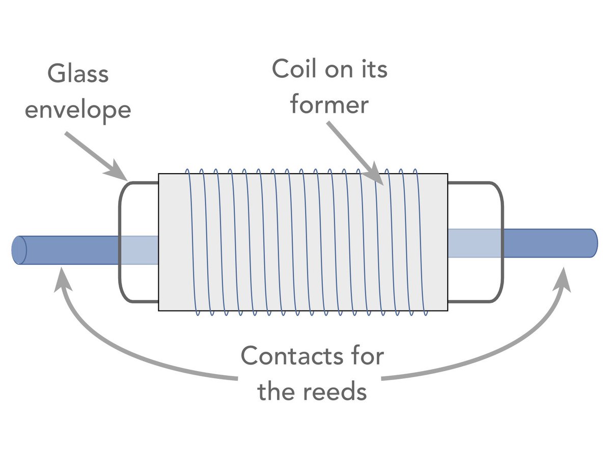
The Amazing Solution for Electronic Switching: The Reed Relay Ever wonder how electronic circuits achieve fast, reliable, and isolated switching without the bulk of traditional electromechanical relays? Meet the reed relay - a compact component that bridges the gap between traditional mechanical relays and solid-state alternatives. What is a Reed Relay? At its core, a reed relay consists of a reed switch - two overlapping nickel-iron blades hermetically sealed inside a glass envelope filled with inert gas (like nitrogen)—wrapped inside an electromagnetic actuating coil. When current passes through the coil, it creates a magnetic field that magnetizes the blades. They attract each other, snap shut, and close the circuit. Remove the current, the field drops, and the spring-loaded contacts snap back apart. Why Engineers Choose Reed Relays: * Speed: Because the gap between contacts is tiny (0.05 to 1 mm), they boast incredibly fast switching speeds—often between 0.5 to a few milliseconds. * Reliability & Longevity: Sealed inside glass, the contacts are entirely protected from moisture, oxidation, and contaminants. * Complete Isolation: They offer absolute physical isolation between the control circuit (coil) and the switched circuit. * Compact Size: They are small enough to fit into standard SIL or DIL integrated circuit packages, saving precious PCB real estate. Design precautions: While they are highly reliable, reed relays aren't always a "set-and-forget" component. When designing them into your circuits, remember: 1. Contact Bounce: The contacts collide with high energy, causing minor "bounces." If switching capacitive or inductive loads, this can cause arcing and reduce contact life. 2. Magnetic Interaction: Unscreened reed relays can experience magnetic coupling. If placed too close together on a PCB, their fields can oppose one another, requiring a higher coil voltage to close. Pro tip: Always look for reed relays with built-in ferrous metal screens to optimize efficiency and enable tight stacking! 3. Current Constraints: They are typically built for low-to-medium signal switching, not heavy-duty power applications. From test and measurement matrix switches to automated telecommunication exchanges, the reed relay remains an elegant, trusted solution for modern hardware engineering. More information- check the link in the comment. #ElectronicsEngineering #HardwareDesign #CircuitDesign #ElectronicComponents #ElectricalEngineering #electronicsnotes
2
4
49
2,130
ElecNotes
Why You NEED An Emitter Follower In this video I explain what an emitter follower circuit is and why you need one in your circuits. These emitter follower amplifiers can be used in many circuits I've used them a huge number of times. In essence, an emitter follower is a common-collector configuration of a bipolar junction transistor or BJT. It's called an "emitter follower" because the emitter voltage closely follows the base voltage, even though there's a small voltage drop across the base-emitter junction. In its very simplest form, the circuit consists of a transistor and an emitter resistor. When a signal is applied to the base, it causes a corresponding current to flow through the collector and emitter. The emitter voltage closely tracks or follows the base voltage, there's just the base emitter junction difference which is about 0.6V for a silicon transistor. I look at the key characteristics of the emitter follower: 1. It has a high input resistance: This means the circuit draws very little current from the input signal source. It reduces the loading on the previous stage. This is typically beta, the transistor current gain times the overall emitter resistance including the load. 2. It has a low output resistance and this makes it suitable for driving lowish-impedance loads. 3. The voltage gain of an emitter follower is unity or 1 and 4. Finally the current gain - this is greater than 1, providing current amplification. I look at where emitter followers are used: a. Their chief use is as a buffer to reduce the load on a source. It could be an oscillator or anything where the loading may be an issue. b. In a similar vein they are used in impedance matching where it's necessary to match the impedance of a high-impedance source to a low-impedance load. The circuits can be directly coupled. Here the bias voltage for the device is taken from the previous stage. Alternatively they can be AC coupled, but here the bias network needs to be set up and the coupling capacitors selected to give the required frequency response. Watch my video now: youtu.be/fSki6td8L4c #emitterfollower #circuitdesign #HardwareDesign #electronicsnotes
3
3
27
1,312
ElecNotes
How to Troubleshoot Bluetooth Pairing Problems We’ve all been there: you turn on your favorite pair of wireless earbuds or set up a Bluetooth speaker, but your phone or laptop simply refuses to acknowledge it even exists. While modern Bluetooth pairing has come a long way, connection hiccups are still incredibly common. Fortunately, the fixes are often very simple. If you or your users are struggling to get wireless gear to cooperate, here is a quick troubleshooting framework to get things connected. The Quick-Fix Checklist Before diving into complex settings, rule out the most common oversights: * Check the battery: Many devices disable their pairing radios if power falls below 10-20%. Plug them in for 15 minutes and try again. * Toggle the radio: Turn Bluetooth off on your phone or laptop, wait 5 seconds, and turn it back on to force background services to restart. * Watch out for interference: Wi-Fi routers, microwaves, and even certain USB 3.0 cables share or disrupt the 2.4 GHz wireless spectrum. Move away from them if you experience a weak link. 2. Master "Pairing Mode" vs. "Power On" One of the most frequent reasons a connection fails is that a device is powered on but not in discoverable pairing mode. When turned on, accessories naturally look for their last connected device. * The Rule of Thumb: If the status light on your speaker or earbuds is solid or blinking slowly, it is not in pairing mode. It must be flashing rapidly to be discoverable. 3. Disconnect from the "Secret" Owner Bluetooth likes exclusivity. If your earbuds are actively connected to a tablet sitting in a drawer nearby, they will completely ignore a new smartphone scan. Turn off Bluetooth on nearby legacy devices to sever the secret connection before trying again. 4. The Golden Rule: Forget, Reset, Re-pair When a connection that used to work suddenly stops, the cached connection data may be corrupted. 1. Forget: Go to your host device settings (iOS, Android, Windows, or Mac) and remove/forget the accessory from your Bluetooth list. 2. Reset: Perform a factory reset on the accessory itself (often done by holding the main button down for 10-15 seconds while in the charging case). 3. Re-pair: Put the accessory back into pairing mode and connect from scratch. For laptop-specific issues, you may also need to check for outdated drivers (Windows Device Manager) or restart the Bluetooth background process via Terminal on a Mac (⁠sudo pkill bluetoothd⁠). What’s your go-to trick when wireless tech refuses to play nice? Let me know in the comments! 👇 Read the full, step-by-step troubleshooting guide in the link in the comments. #Bluetooth #WirelessTechnology #Troubleshooting #TechTips #ElectronicsNotes #TechSupport
2
3
20
1,288
ElecNotes
Calling all Radio Amateurs and CW Enthusiasts! Whether you are a seasoned operator working the bands or just appreciate the heritage of wireless communication, we’ve got the perfect addition to your shack. Our Morse Code Mug is more than just a place for your morning coffee—it’s a functional tribute to the art of CW. Featuring a clear, concise reference guide for the Morse code alphabet, it’s the ideal companion for those long nights on the air or simply to display your passion for radio history. Why you'll love it: * A Daily Reference: Keep the code at your fingertips (or your lips!) while you're at your desk. * Made for the Shack: A durable, high-quality design that fits perfectly alongside your transceiver and key. * The Perfect Gift: Whether you’re buying for yourself or a fellow ham, it’s a great conversation starter. It's a small way to celebrate the skill and precision that keep Morse code thriving in the modern era. 👉 Grab yours here: electronics-notes-shop.fourt… Let’s keep the spirit of CW alive—one cup of coffee at a time! #AmateurRadio #HamRadio #hamr #MorseCode #CW #RadioOperator #ElectronicsNotes #Radiostation #RadioHobbies #ElectronicComponents
2
5
13
1,245
ElecNotes
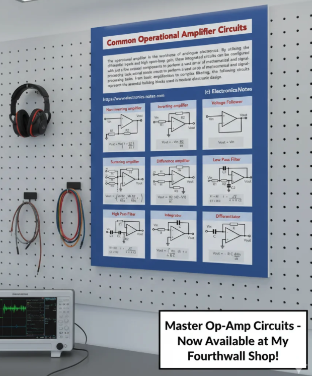
Master your circuit design: Essential Op-Amp circuits at your fingertips! Whether you're a student building your first lab project or an experienced engineer needing a quick refresher, keeping the fundamentals handy is a game-changer. Operational amplifiers are the building blocks of modern analog electronics—but remembering every configuration and formula can be a challenge. That’s why I’ve created a Common Op-Amp Circuits Crib Sheet. This downloadable infographic is designed to be your go-to reference for the circuits you use every day, including: * Inverting & Non-Inverting Amplifiers * Voltage Followers * Summing Amplifiers * Active Filters & Integrators * Essential Gain and Formula references Why this crib sheet? * Clear & Concise: Designed to give you the information you need at a glance. * Perfect for the Bench: Keep it digitally on your tablet or print it out to keep right next to your breadboard. * Time-Saver: Stop searching through bulky textbooks when you need to calculate gain or identify a pinout. Cut down your design time and keep your focus on the innovation, not the lookup. 👉 Get your copy here: electronics-notes-shop.fourt… #ElectronicsEngineering #OpAmps #CircuitDesign #AnalogElectronics #EngineeringStudent #PCBDesign #ElectronicsNotes #Prototyping #EngineeringResources
4
36
1,383
ElecNotes
The 2N2222: Greatest Transistor Ever? My latest short video I check out the legendary 2N2222 transistor, sometimes called the 2N quad 2 transistor. The 2N2222 was introduced back in 1962 and at its introduction, it became legendary transistor because it offered performance unequalled by any other transistor of its time. The 2N2222 was used primarily as a switching transistor, but it was also widely used as a general purpose transistor and was found in a huge number of electronic circuits. Check out my video now: youtube.com/shorts/APiLk1BnH… #2N2222 #transistor #switchingtransistor #electroniccomponents #techhistory #historyoftechnology #electronicsnotes
1
2
29
1,210
ElecNotes
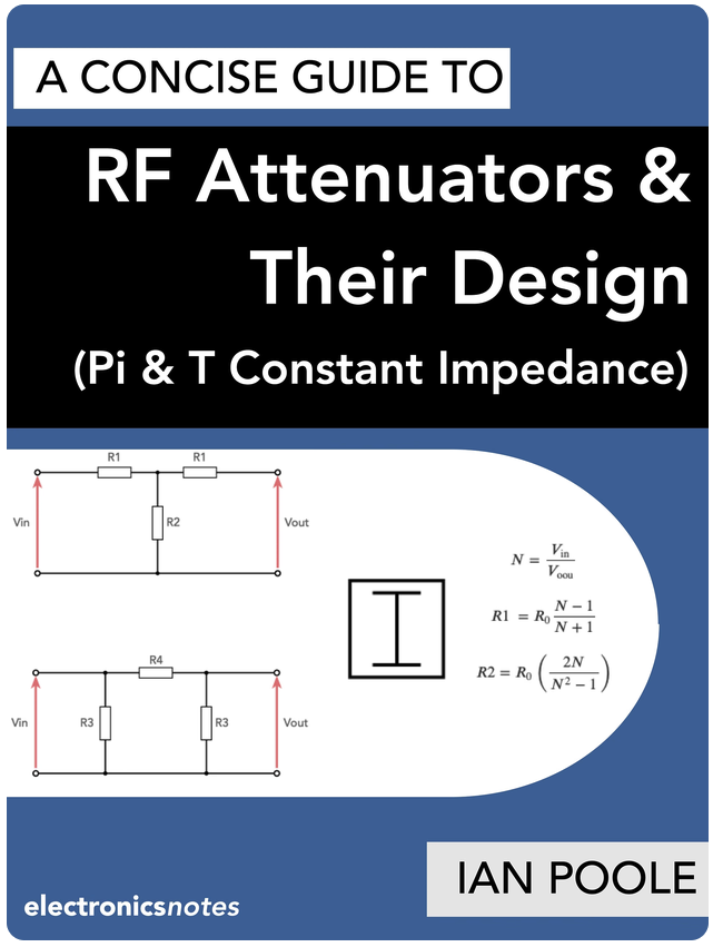
RF Engineering: Struggling with signal levels? Get the clarity you need. In RF circuit design, managing signal levels is everything. Whether you are matching stages, preventing amplifier saturation, or simply calibrating power levels, the RF Attenuator is one of the most fundamental tools in your arsenal. But how do you move from the theory of Pi and T-networks to a practical, production-ready design? I’ve put together a resource designed to cut through the noise: "A Concise Guide to RF Attenuators & Their Design." Why this guide is a must-have: * The Theory, Simplified: Understand the core concepts behind resistive attenuator networks without getting lost in overly academic jargon. * Practical Design Steps: Step-by-step guidance on calculating component values for common configurations, including Pi, T, and Bridged-T networks. * Performance Considerations: Learn about the impacts of frequency, impedance matching, and physical layout—critical factors that can make or break an RF design. * Compact & Focused: This isn't a 500-page textbook. It’s a concise, actionable guide built for engineers and students who need results, fast. Whether you are designing for test equipment, radio systems, or broad-band applications, this guide serves as a perfect reference for your engineering library. Stop guessing your values and start designing with confidence. 👉 Download your copy today: electronics-notes-shop.fourt… #RFEngineering #RadioFrequency #CircuitDesign #ElectronicsEngineering #WirelessTechnology #EngineeringResources #ElectronicsNotes #RFDesign
24
97
3,390
ElecNotes
The Origins the Smith Chart: How this RF Engineering Essential was Developed. If you’ve ever designed an RF circuit or used a Vector Network Analyzer (VNA), then most likely you’ve seen or used a Smith Chart. These charts are an incredible way of visualising complex impedances and their matching. But did you know that what we now consider a universal standard was actually a "photo-finish" invention developed simultaneously across the globe? A Global Race for Clarity In the late 1930s, engineers were drowning in the complex mathematics of transmission lines. The "Smith" chart was actually a triple-threat discovery: • 1937: Tōsaku Mizuhashi (Japan) and Amiel R. Volpert (Russia) both proposed similar concepts. • 1939: Phillip H. Smith (USA) published his version, which ultimately became the global standard. From "Transmission Line Chart" to Household Name Phillip Smith didn’t set out to put his name on every RF VNA screen and more in the world. He originally called his invention the "Transmission Line Chart." The shift happened at MIT’s Radiation Laboratory during the 1940s. Early adopters found the tool so indispensable that they began referring to it simply as "The Smith Chart." By the time Smith realized his name was synonymous with impedance matching, the name had already stuck. From Paper to Pixels For over a decade, the chart existed only on paper. It wasn't until 1950 that the world saw a Smith Chart on an actual instrument screen, thanks to the Rohde & Schwarz Z-g Diagraph. Today, it is a standard digital interface on every VNA, proving that great design—even when it's nearly 90 years old—never goes out of style. Link to more information on my website also in the comments. 👇 #RFEngineering #ElectricalEngineering #HistoryOfTech #SmithChart #RFdesign #WirelessDesign #EngineeringHistory #electronicsnotes
2
21
111
3,957
ElecNotes
Selecting the Best Op-Amp for Your Circuit Design In circuit design, the "ideal" op-amp (infinite gain, zero noise, infinite bandwidth) doesn't exist. Instead, successful engineering is about finding the right balance between performance, availability, and cost. Whether you're building a precision integrator or a simple buffer, here’s a quick guide on how to navigate your selection, inspired by the deep dive over at Electronics-Notes: 🔹 Assess Your Primary Need: * High Input Impedance: If you’re working with sensors or integrators where charge leakage is a concern, look for **FET-input** op-amps. * Low Noise: Crucial for the initial stages of a signal chain. Remember, noise added at the start gets amplified by every subsequent stage. * Low Power: Essential for battery-operated devices. Look for "micropower" versions that trade off speed for longevity. * Rail-to-Rail: If your supply voltage is low (e.g., 3.3V), ensure your op-amp can handle swings close to the supply rails. 🔹 Think Beyond the Specs: * Packaging: Do you need breadboard-friendly DIP-8 or space-saving SMT? Don't forget that dual or quad packages can save board space, but they often lack offset null pins. * Availability & Sourcing: For commercial projects, "jellybean" parts (like the classic LM358 or UA741) are easier to source and often have multiple manufacturers, reducing supply chain risks. * Lead Times: Sometimes the "best" chip is the one you can actually get delivered by your distributor today! Pro Tip: Don't over-specify. Increasing performance requirements unnecessarily can inflate costs and restrict your supplier options. For more information check out the link in the comments. #ElectronicsEngineering #CircuitDesign #HardwareDesign #OpAmp #EngineeringTips #ElectronicsNotes
2
6
29
1,361
ElecNotes
Leadership News: Avnet Silica announces Maryannick Dauba as President. Avnet Silica has appointed long-standing leader Maryannick Dauba as President, effective today, July 1, 2026. With over 15 years of experience within the organization, Maryannick brings a wealth of expertise across sales, business engagement, and customer-facing operations. Her previous leadership roles include EMEA Vice President of Business Engagement, EMEA Sales Vice President, and Regional Vice President for South Europe. This appointment underscores Avnet Silica’s commitment to continuity and long-term, customer-focused growth across the EMEA region. “Maryannick combines deep knowledge of our customers, suppliers and organisation with extensive leadership experience across Avnet Silica,” said Gilles Beltran, President, Avnet EMEA. “She understands what makes this business successful and is well positioned to lead its continued growth across EMEA”. Reflecting on her new role, Maryannick noted the strength of the organization’s relationships and expertise. "I look forward to building on that foundation and continuing to support our customers and supplier partners as we grow the business together". Please join us in congratulating Maryannick Dauba on her new role as she leads Avnet Silica into its next phase of strategic growth! #AvnetSilica #Leadership #ElectronicsIndustry #Semiconductors #BusinessGrowth #EMEA #CareerNews #electronicsnotes
4
619
ElecNotes
Function moves to the surface: binder is redefining component design. The industry trend of decentralization is taking a massive leap forward. Instead of cramming more circuit boards and separate sensors into a housing, binder is now printing electronic functionality—conductors, heating elements, and sensors—directly onto the surfaces of 3D components. Breaking the limits of traditional assembly: Conventional assembly technology is increasingly hitting a wall as devices get smaller, more connected, and more sensor-intensive. Every extra component is a potential point of failure and a space-waster. binder’s approach at their Innovation and Technology Center (ITZ) changes the game by applying functional layers directly onto materials like plastic, metal, glass, or ceramic. Key Benefits: * Design Freedom: Seamless functionality on curved or irregularly shaped surfaces where conventional circuit boards simply can’t fit. * Efficiency: Significant reduction in individual parts, assembly steps, and overall system weight. * Application Versatility: From predictive maintenance sensors in mechanical engineering to touch interfaces and integrated heating elements. From Prototype to Series Production: What sets binder apart is the ability to take these printed concepts beyond the research stage. While the ITZ focuses on developing these high-precision printing processes, the broader binder group handles the full, production-ready system integration—combining printed layers with connectors and connection technology to deliver a complete, seamless solution. "Printed electronics shifts the limit of what a single component can achieve," says Dr.-Ing. Martin Ungerer, Team Leader Printed Electronics at binder ITZ. If you are looking to integrate advanced functionality into the smallest of spaces, binder is positioning itself as a vital development partner for the next generation of industrial devices. #Innovation #PrintedElectronics #IndustrialDesign #Engineering #SmartComponents #binderGroup #Manufacturing #Industry40 #TechTrends #electroniccomponents #electronicsnotes
9
930
ElecNotes
Antenna Feed Impedance: the Secret to Antenna Efficiency? We all like our antennas to be as effective as possible. One key aspect is the reflected power. The connection between the transmitter and antenna is key. The feed impedance of an antenna isn't just a single number; it’s a complex combination of resistance, capacitance, and inductance. To get maximum power transfer, your feeder must match this impedance perfectly. Here are the 3 critical components you need to know: 1. The Two Faces of Resistance • Radiation Resistance: This is the "good" resistance. It represents the power successfully converted into radio waves. For a half-wave dipole in free space, this is typically around 73Ω. • Loss Resistance: This is the "bad" resistance. It’s the power lost as heat due to the resistance of the antenna conductors. At high frequencies, the skin effect makes this even more challenging! 2. The Role of Reactance Antennas act like tuned circuits. At resonance, the inductive and capacitive elements cancel out, leaving only pure resistance. But move away from that resonant frequency, and your impedance will quickly become inductive or capacitive, leading to a mismatch. 3. External Factors That Change Everything Your antenna doesn’t live in a vacuum. Its impedance is heavily influenced by: • Proximity to objects: Adding directors or reflectors (like in a Yagi antenna) can drop a dipole’s impedance from 73Ω to 20Ω or less. • Height above ground: The ground acts as a giant reflector that shifts your impedance levels. • Feed Point: Where you connect matters. Center-feeding a dipole gives low impedance, while end-feeding results in very high impedance. The Bottom Line: To achieve high Antenna Efficiency, you want to maximize Radiation Resistance while minimizing Loss Resistance. When your feeder (typically 50Ω or 75Ω) matches the antenna, you avoid standing waves (VSWR) and ensure your signal actually makes it "into the ether." How do you handle impedance matching in your designs? Do you prefer Baluns, Gamma matches, or strictly resonant designs? Let’s discuss in the comments! 👇 Check out my link in the comments. #RFDesign #AntennaTheory #WirelessComms #ElectricalEngineering #ElectronicsNotes #hamradio #amateurradio #hamr
1
7
44
1,568
ElecNotes
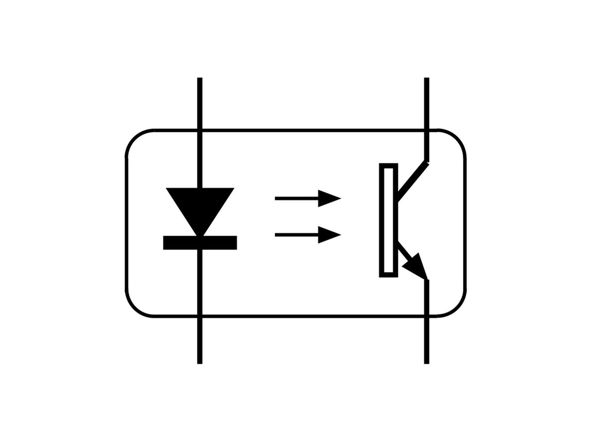
Key Components Highlight: The Optocoupler Optocouplers are an ideal way of isolating two circuits while passing data from one to the other. Optocouplers can be described by a variety of different names including optoisolator, and photocoupler. Essentially an optocoupler or photocoupler is a semiconductor device that uses a short optical path or link to couple a signal from one electrical circuit to another whilst providing electrical isolation. The photocouplers or optocouplers are typically contained in a single package, often about the size of an integrated circuit, although there is a large degree of variation according to the intended application. When selecting an optocoupler for your next project, keep these 3 key specs in mind: 🔹 Current Transfer Ratio (CTR): The ratio of output current to input current. This varies wildly—from 10% to 5000%—depending on whether you use a phototransistor or a photodarlington. 🔹 Bandwidth: Crucial for data transmission. Standard phototransistors often peak around 250 kHz, so choose wisely for high-speed data! 🔹 Isolation Voltage: Ensuring the package can handle the potential difference between your input and output stages. I’ve put together a comprehensive guide covering everything from internal symbols to the differences between optos and solid-state relays. #ElectricalEngineering #PCBDestign #Optoelectronics #TechTips #optocoupler #optoisolator #photocoupler #electronicsnotes #electroniccomponents
1
1
28
1,172
ElecNotes
Bluetooth Explained: what it is, how it works & the Viking connection. How do your wireless earbuds, smartwatch, and car actually connect? It’s Bluetooth which is everywhere in our modern world, but the story behind this invisible "wire" is surprisingly deep. In this video, we dive into the fascinating origins, engineering, and science behind Bluetooth technology. From a 10th-century Viking king to a Hollywood actress, the history of Bluetooth is as clever as the tech itself. What you’ll learn in this video: * Viking Connection: Discover why this modern protocol was named after a 10th-century Scandinavian king and how that shaped the iconic logo. * The Hedy Lamarr Legacy: Learn how a 1940s Hollywood film star co-invented the "Frequency Hopping" technology that keeps your Bluetooth signal from dropping out today. * How it Actually Works: A plain-English breakdown of the 2.4 GHz radio band and why hopping between frequencies thousands of times a second is the secret to a stable connection. * Bluetooth Classic vs. BLE: We demystify the two main "flavours" of Bluetooth—why we need "Classic" for high-quality audio streaming and why "Bluetooth Low Energy" (BLE) is the absolute game-changer for the Internet of Things (IoT) and wearable battery life. Whether you're an engineering student, a tech enthusiast, or just curious about how your gadgets talk to each other, this deep dive provides the perfect summary of the standard that unites our digital lives. Check out my video now: youtu.be/KOOXkRa3big #Bluetooth #bluetoothwireless #frequencyhopping #Bluetoothconnectivity #electronicsnotes
1
21
1,126
ElecNotes
Top tips for using aluminium electrolytic capacitors Electrolytic capacitor can have a bad name for reliability, but if used well, they can provide very reliable service. If some top tips are followed, then they can be a very good choice for a capacitor. Aluminium electrolytic capacitors do degrade with time. Many electrolytics have a vent for allowing excess gasses to escape. This escape can result in the electrolyte drying out and the performance of the capacitor falling. Also if aluminium electrolytic capacitors are left for a few years, then the oxide layer on the anode can dissipate. When this happens the capacitor needs to be repolarised. This can be done by applying a current limited voltage to the capacitor. Initially the leakage current across the capacitor will be relatively high and then it will fall as the oxide layer forms. It is also wise to take precautions to prolong the life of the capacitor, and ensure the best overall reliability. Below are our golden tips to maximise the life of an aluminium electrolytic capacitor and ensure the best reliability: •Understand the essentials of electrolytic capacitors, discover their benefits & understand how they can be used to provide high levels of capacitance with high reliability with our top tips. •Run within its voltage limits:   It is always wise to run any component with a good margin below the maximum ratings. Many companies state in their design rules that for electrolytic capacitors, they should only be run at about 50% of their maximum ratings to ensure optimum reliability. If the maximum limits are exceeded then leakage current levels will rise and there is the possibility of localised breakdown leading to an explosive failure of the component. •Keep within its current rating:   In many applications an electrolytic capacitor will be required to provide high levels of ripple current. This is to be expected in applications like being used as a smoothing capacitor in a power supply. Ii is imperative to ensure that the capacitor can withstand the current being required from it. Check that the capacitor is operating within its current limits and is not becoming too warm in operation. •Never reverse bias the capacitor:   When run under a reverse bias, the leakage levels will be very much higher than in the forward direction. Again this can lead to catastrophic breakdown and failure. •Keep temperatures down:   Heat shortens the life of any aluminium electrolytic capacitor. A good rule of thumb is that every 10°C over 85°C will halve the life expectancy of the component. •Only for lower frequencies:   Electrolytic capacitors are not good when used at higher frequencies. Typically they are limited to frequencies up to a maximum of around 100kHz. These tips will help ensure that the best performance is obtained when an electrolytic capacitor is used in an electronic circuit design, and also that they are chosen when they are the best option for the given situation. #capacitors #electrolyticcapacitors #circuitdesign #HardwareDesign #electronicsnotes #electroniccomponents
2
4
34
1,520
ElecNotes
Transistor Common Emitter Amplifier - the most versatile circuit? The transistor common emitter circuit configuration is used for transistor circuit design. But how useful really is it? In this video, I explain all about the common emitter amplifier: what it is, its advantages and see some circuit designs. The transistor common emitter amplifier is probably the most widely used transistor configuration. First of all, I explain what the Common Emitter Amplifier actually is: it's a circuit that uses a transistor, to amplify an input signal. The "common emitter" part refers to the fact that the emitter terminal is common to both the input and output circuits. Next I look into how it works: when a small input signal is applied to the base of the transistor, it causes a much larger current to flow through the collector to the emitter. This results in a significant amplification of the input signal. Here's a list of its chief characteristics: a) It has a high voltage gain making it ideal for various applications. b) It offers a moderate input impedance, allowing it to be driven by a variety of signal sources. c) It has a medium output impedance and this makes it suitable for driving many loads. Where is it used? 1) As general amplifiers for amplifying everything from audio signals, to almost anything. 2) In RF circuits for amplifying signals in communication systems in both transmitters and receivers 3) They can even be configured as oscillators by providing the right kind of feedback. The common emitter amplifier is a versatile and fundamental circuit in electronics. Its ability to amplify signals effectively makes it an essential component in numerous electronic devices. Check out my video now: youtu.be/A0sWlW1o0h0 #transistor #commonemitter #amplifier #circuitdesign #HardwareDesign #HardwareEngineering #electronicsnotes
9
52
1,780
ElecNotes
Why your Linear Power Supply needs a Reservoir Capacitor The smoothing capacitor is used to convert the "bumpy" rectified AC into the smooth DC required by sensitive electronics. The capacitance and period the soothing capacitor are crucial. In both linear and switch-mode power supplies, the rectifier output consists of a series of half-sine waves. Without smoothing, digital circuits would lose power every half-cycle, and analog circuits would be plagued by hum and noise. Here are 3 key takeaways for engineers and hobbyists on getting smoothing right: 1️⃣ The "Fill in the Gaps" Strategy: A reservoir capacitor (typically an aluminum electrolytic) works by charging up at the voltage peak and discharging into the load when the rectifier voltage drops. Essentially, it "fills in the dips" to maintain a steady output. 2️⃣ Full-Wave vs. Half-Wave: Efficiency matters! Full-wave rectification is always preferable because the gaps between peaks are shorter. This leads to significantly better smoothing and allows for a smaller capacitor to achieve the same ripple voltage. 3️⃣ Don't ignore Ripple Current! When choosing a capacitor, capacitance and voltage aren't the only specs that matter. You must check the Maximum Ripple Current. * Because the capacitor only charges during a very short window of the cycle, the peak charging current can be much higher than the steady-state load current. * Overlooking this leads to overheating, reduced lifespan, or even catastrophic failure. Pro-tip for the maths: To estimate peak-to-peak ripple Vripple for a full-wave rectifier, use: 👉 Vripple = Iload / (2  f  C) Looking to go deeper into the calculations and filters? Check out the full breakdown on Electronics-Notes: electronics-notes.com/articl… #ElectronicsEngineering #PowerSupply #CircuitDesign #ElectricalEngineering #electronicsnotes #electroniccomponents  #LearningElectronics
7
26
1,624