Filter
Exclude
Time range
-
Near
ElecNotes
Op-Amp Design: The Gain & Bandwidth Balance If you’ve ever had a situation where your high-gain amplifier response is "rolling off" sooner than expected, it’s likely you are encountering the Gain-Bandwidth Product (GBP) limits. In voltage feedback operational amplifier design, there is a fundamental trade-off: The more gain you want, the less bandwidth you get. Based on the insights from my Electronics-Notes website, here are three essential takeaways for your next analogue design: 1️⃣ The Open-Loop Reality: Most voltage-feedback op-amps (like the classic 741) have a surprisingly low open-loop breakpoint—sometimes as low as 6Hz! Beyond this point, the gain drops at a steady rate of -20dB/decade. 2️⃣ The GBP Constant: For standard voltage-feedback amplifiers, the Gain x Bandwidth remains constant. If you decrease your gain by a factor of 10, you gain a factor of 10 in bandwidth. It’s a literal balancing act. 3️⃣ Why Compensation Matters: Why is the bandwidth so limited? Internal frequency compensation is built into most ICs to ensure stability. Without it, your amplifier might turn into an oscillator! Pro-Tip: If your application requires high gain and high bandwidth simultaneously, you might need to move away from voltage-feedback op-amps and look into Current Feedback architectures, which don't follow the same linear GBP relationship. Are you hitting bandwidth bottlenecks in your current projects? Let’s discuss in the comments! Also for more details check out my website - link in the comments. #ElectronicsEngineering #CircuitDesign #AnalogDesign #OpAmps #HardwareDesign #EngineeringEducation #electronicsnotes
1
3
34
966
PCBsync
MLCC capacitors are nonlinear. Here’s how to model it in LTspice (and why it saved me from using expensive film caps). Most engineers know Class‑2 MLCCs (X5R, X7R) lose capacitance under DC bias. A “10 µF” part can easily drop to 5 µF or less at 5 V. But the real kicker? If the voltage across the capacitor changes over time, so does the capacitance. That makes it nonlinear—and that can distort analog circuits. I ran into this while designing an analog feedback controller for temperature regulation. Thermal systems are slow, so the op‑amp loop needed a very large time constant—several µF in the feedback network. Ideally I’d use C0G/NP0 or film capacitors (very linear). But µF‑range C0G is rare, large, and expensive. An X5R MLCC looked attractive—if the nonlinearity didn’t destabilize my loop. Here’s how I modeled it in LTspice: Samsung publishes DC‑bias curves. I fitted the data for a 3.3 µF MLCC with: C(V) = (C0 - Cmin) * (Vk² / (V² Vk²)) Cmin LTspice models nonlinear caps via stored charge Q(V). Integrating the above gives: Q(V) = Vk*(C0 - Cmin)*atan(V/Vk) Cmin*V LTspice automatically computes C(V) = dQ/dV. What the simulation showed: A simple op‑amp integrator with a square‑wave input should produce a triangle wave. With an ideal capacitor → perfect triangle. With the X5R model → the ramp slope changes as capacitance varies with voltage → distorted output. The bottom line for my thermal controller: Despite the distortion, the loop remained stable with the X5R. I saved cost and PCB space by avoiding a film capacitor. 👉 If you’re using large MLCCs in analog feedback paths, don’t assume linearity. Model it. You might be pleasantly surprised. #LTspice #AnalogDesign #MLCC #Capacitors #Engineering #CircuitDesign
48
MicrochipTech
Clean data starts with a quiet signal path. MCP6071x precision op amps support confident measurement across industrial, medical, and automotive designs—where accuracy drives outcomes. mchp.us/4wdCD9z #AnalogDesign #EmbeddedSystems #HighAccuracy #AnalogInnovation
1
2
11
1,302
SSCSociety
Will AI replace analog designers? 🤖 Or will it help us innovate faster? Join industry legend Dr. Behzad Razavi (UCLA) as he evaluates AI's capabilities against the 5-level analog design pyramid. 👇 Link: bit.ly/3QAA4yu #IEEESSCS #CircuitDesign #AnalogDesign
2
4
136
PCBsync
Input capacitors in DC/DC regulators: the often-overlooked root cause of output instability. ⚡ Input Capacitor Design for DC/DC Regulators — Part 1: Ceramic & Bulk Capacitors Input capacitor selection is one of the most underestimated aspects of DC/DC regulator design — yet it has a direct impact on whether your converter remains stable under real operating conditions. Get it wrong, and you may find yourself spending hours troubleshooting what looks like a control loop issue, when the real culprit is sitting right at the input. In Part 1, I cover: The ceramic bulk capacitor strategy Key sizing equations Why the input and output are more closely coupled than most engineers realize 🔜 Part 2 is coming soon — including a failure mode that catches even experienced engineers off guard. #PowerElectronics #DCDC #BuckConverter #PCBDesign #HardwareEngineering #AnalogDesign #EmbeddedSystems #EMC #PowerSupplyDesign
9
RaymingTech
Input capacitors in DC/DC regulators: the often-overlooked root cause of output instability. ⚡ Input Capacitor Design for DC/DC Regulators — Part 1: Ceramic & Bulk Capacitors Input capacitor selection is one of the most underestimated aspects of DC/DC regulator design — yet it has a direct impact on whether your converter remains stable under real operating conditions. Get it wrong, and you may find yourself spending hours troubleshooting what looks like a control loop issue, when the real culprit is sitting right at the input. In Part 1, I cover: The ceramic bulk capacitor strategy Key sizing equations Why the input and output are more closely coupled than most engineers realize 🔜 Part 2 is coming soon — including a failure mode that catches even experienced engineers off guard. #PowerElectronics #DCDC #BuckConverter #PCBDesign #HardwareEngineering #AnalogDesign #EmbeddedSystems #EMC #PowerSupplyDesign
8
49
1,711
RaymingTech
🔌 Analog Circuit Design Interview Series — Question #2: Signal Swing One concept that separates good analog designers from great ones? Understanding signal swing. Signal swing defines the maximum undistorted output voltage range an amplifier can deliver. Push beyond it, and your transistors fall out of saturation — leading to gain compression, harmonic distortion, and a signal your downstream circuit won't thank you for. In short: no swing = no linearity. 🧠 Try this problem: Given a PMOS amplifier stage with the following parameters: VDD = 5 V | VGG = 3.5 V | Vtp = −1 V | Kp = 1 mA/V² | λ = 0 What is the maximum symmetrical output voltage swing? Drop your approach or answer in the comments 👇 — whether you're a student prepping for interviews or a seasoned engineer, I'd love to see how you think through it. 💡 Mastering signal swing isn't just about passing interviews — it's fundamental to designing amplifiers that actually work in the real world. Follow for more analog design interview questions every week. #AnalogDesign #CircuitDesign #VLSI #InterviewPrep #Electronics #Engineering #EmbeddedSystems #SemiconductorDesign
2
199
ElecNotes
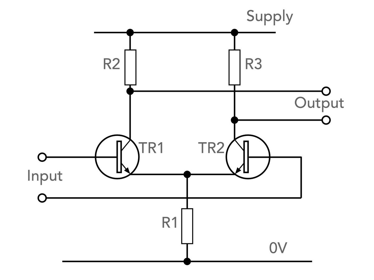
Why the "Differential Amplifier" is the Hero of Modern Electronics If you’ve ever looked at the internal schematic of an Operational Amplifier (Op-Amp), you’ve seen it: the Transistor Differential Amplifier, also known as the Long-Tailed Pair (LTP). But why is this specific configuration so critical to analog design? Derived from the brilliant work of Alan Blumlein in the 1930s, the LTP transitioned from vacuum tubes to transistors to become the fundamental building block of high-performance amplifiers. Here’s why it’s a design "must-know": 🔹 Differential Gain vs. Common Mode Rejection: The circuit’s superpower is its ability to amplify the difference between two signals while ignoring noise that is common to both. This is quantified by the Common Mode Rejection Ratio (CMRR). High CMRR is the reason your audio and data cables can run through noisy environments without losing signal integrity. 🔹 The "Long Tail" Secret: The performance of the circuit relies on the "tail" resistor (or constant current source) connected to the emitters. The higher the impedance of this tail, the better the balance and the higher the CMRR. In ICs this is typically replaced by an active current source for better performance. 🔹 Symmetry is King: Because the circuit uses two matched transistors, it is inherently stable against temperature fluctuations. If the temperature rises, both transistors are affected equally, keeping the output balanced. From precision instrumentation to high-fidelity audio and integrated circuits, the Long-Tailed Pair remains as relevant today as it was 80 years ago. What are your experiences with this circuit? Let me know in the comments. Check out the link in the comments for more information. #ElectronicsEngineering #AnalogDesign #CircuitDesign #Transistors #ElectricalEngineering #TechHistory #electronicsnotes
8
47
310
10,280
ElecNotes
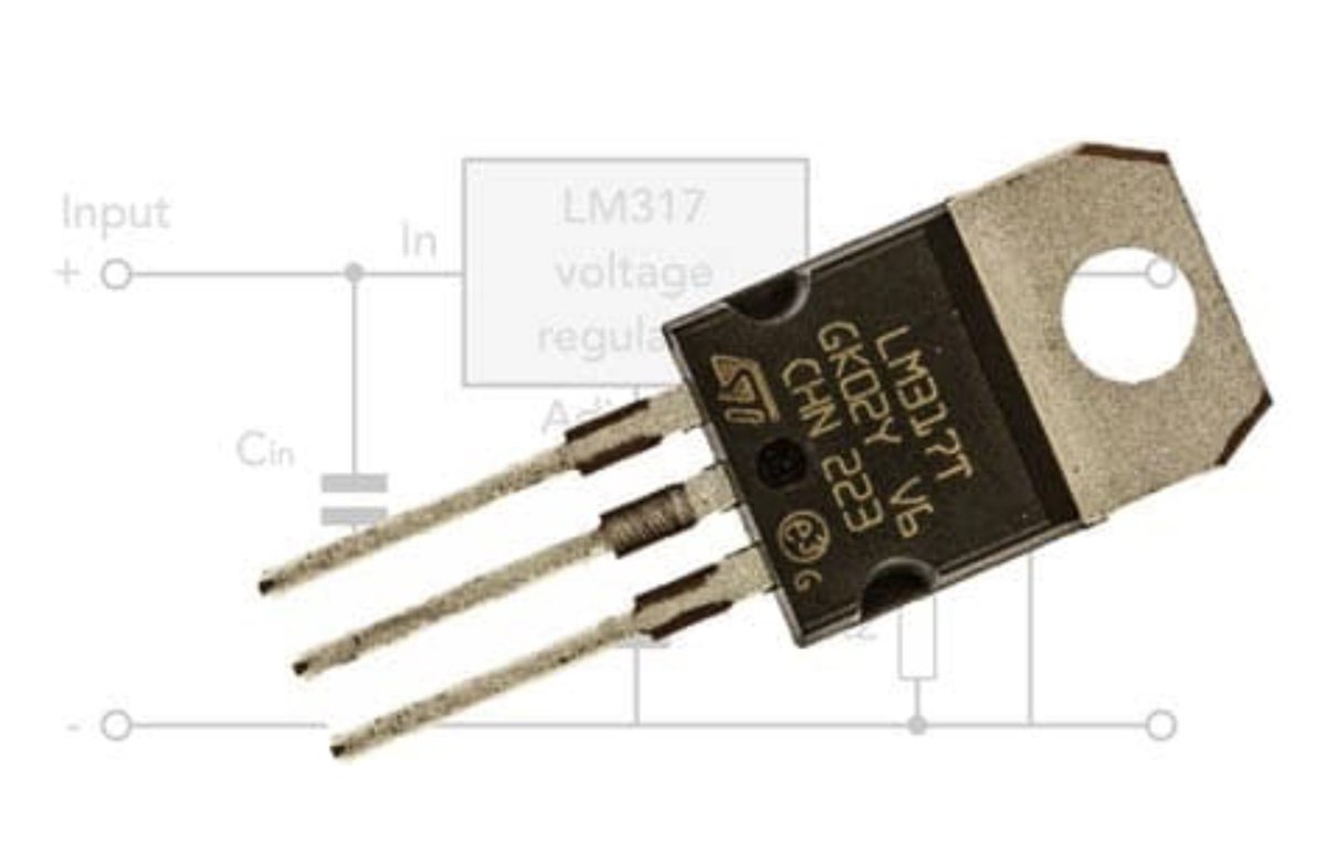
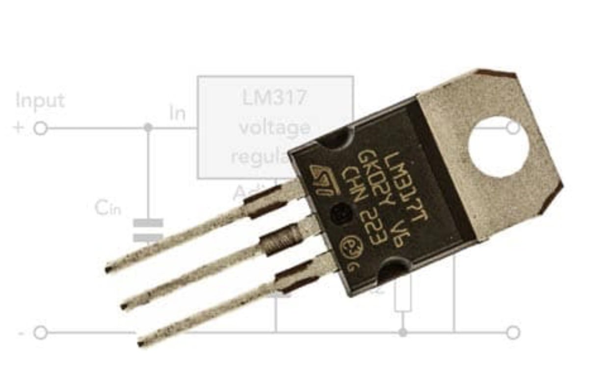
Why the LM317 Voltage Regulator Chip Still Rules When you are looking for a straightforward voltage regulator chip, sometimes the classic solutions are still the best. The LM317 adjustable voltage regulator has been a staple on engineer workbenches for decades - many might refer to it as a jellybean regulator chip. Whether you're building a variable lab supply, a constant current source for LEDs, or local on-card regulation, this 3-terminal wonder is as versatile as it is reliable. It’s cheap, plentiful and as it’s been around for ages it’s available from many suppliers. Based on information on my website , here is why the LM317 should still be in your component drawer: Key Features • Wide Output Range: Adjusts from 1.2V all the way up to 37V. • High Current Capability: Capable of delivering over 1.5A with proper heatsinking. • Floating Regulator: Because it doesn't have a dedicated ground pin, it can be used in high-voltage applications as long as the input-to-output differential is maintained. • Robust Protection: Built-in current limiting and thermal overload protection make it incredibly "forgiving" during the prototyping phase. Pro-Tips for a Stable Circuit To get the best performance out of your LM317 design, keep these practical tips in mind: 1. Capacitors are NOT optional: Use a 0.1µF ceramic on the input to handle line impedance and a 1µF tantalum on the output to ensure transient stability. 2. The "Protection Diode" Trick: If you’re using large output capacitors (over 25µF), add a protection diode from output to input. This prevents the capacitor from discharging back through the IC if the input is shorted. 3. Layout Matters: Keep your programming resistors as close to the IC terminals as possible to minimize voltage drops that can degrade regulation. 4. Heatsink Connection: Remember that on the TO-220 package, the metal tab is internally connected to the Output pin, not ground! Always use an insulator kit if mounting to a common chassis. The LM317 is a testament to the idea that good analog design is timeless. It’s cheap, widely available, and virtually impossible to make obsolete. For more information check out my website - link in the comments. Are you still using the LM317 in your modern designs, or have you fully switched to LDOs and Switchers? Let’s talk shop in the comments! 👇 #ElectronicsEngineering #AnalogDesign #PowerSupply #LM317 #ElectricalEngineering #MakerMovement #CircuitDesign #electronicsnotes
4
11
115
4,043
MuhumuzaWarren
Most op amps are not designed for femtoamp currents. Electrometer amplifiers are a completely different class. We are talking about fA input bias currents, TΩ source impedances, PCB leakage currents, and humidity induced measurement drift. #Electronics #AnalogDesign #PCBDesign
2
20
ElecNotes
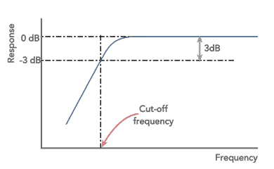
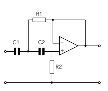
High Pass Active Filter Design: Simplified with Op-Amps! Looking to eliminate low-frequency hum or noise from your analogue circuits? Using an Operational Amplifier (Op-Amp) is one of the most effective ways to build a high-performance high-pass filter without the need for bulky inductors. I’ve put together a comprehensive guide on designing Active High Pass Filters, focusing on the popular Butterworth response—known for its flat passband and straightforward design equations. Key Highlights: ✅ Why Active? Unlike passive filters, op-amp circuits provide gain (if needed) and prevent signal loading due to their high input impedance. ✅ Single-Pole vs. Two-Pole: Learn how a single capacitor/resistor pair gives you 6dB/octave, or step up to a Sallen-Key configuration for a sharper 12dB/octave roll-off. ✅ Design Shortcuts: For a 2-pole Butterworth response with unity gain, the math is surprisingly simple! * Set R_1 = R_2 * Set C_1 = 2 . C_2 * Calculate your cut-off frequency: f = √2 / (4 π R C2) Pro-Tips for Your Build: 📍 Resistor Selection: Aim for 10kΩ to 100kΩ to keep output impedance stable. 📍 Capacitor Choice: Avoid electrolytic capacitors! Stick with Ceramic or Plastic Film for better tolerance and stability. 📍 Cascading: Need a steeper slope? You can cascade these stages to achieve 24dB, 36dB, or higher roll-off rates. Dive into the full circuit diagrams and component selection guide here: 🔗 electronics-notes.com/articl… #ElectronicsEngineering #CircuitDesign #OpAmps #AnalogDesign #ElectricalEngineering #EngineeringTips #ElectronicsNotes
5
57
1,643
Newark_Avnet
Power your next design with ST’s latest analog innovations. New mid‑voltage DC‑DC solutions and a broad portfolio of industrial & automotive‑ready analog products are in stock now: bit.ly/4uzhEfR #STMicroelectronics #AnalogDesign #PowerElectronics
1
3
79
ElecNotes
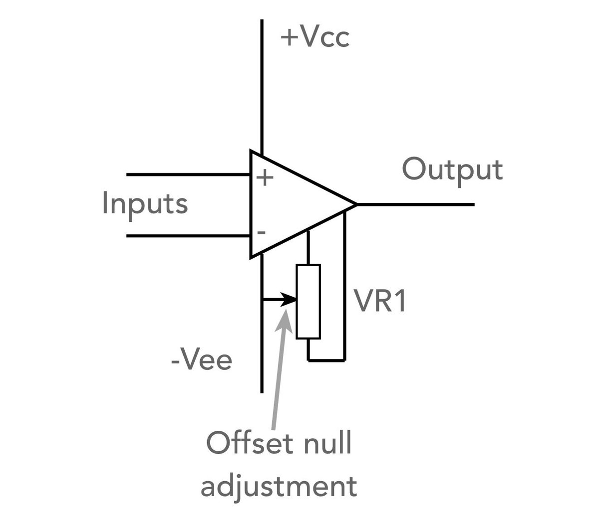
Op-Amp Offset Null: what it is and where to use it! If you’ve ever shorted the inputs of an operational amplifier and still seen a voltage at the output, you’ve encountered Input Offset Voltage. It’s not just seen when you short the inputs - it’s very important when amplifying low level signals like those you see from sensors. In a perfect world, an op-amp is a balanced differential amplifier. In the real world, tiny mismatches in the internal transistor pairs, collector resistors, or current gains (β) during manufacturing create an inherent imbalance. While this might not matter in AC-coupled circuits, for DC amplifiers, instrumentation, and sensor applications, it’s a critical challenge. Any small offset at the input is amplified by the gain of the circuit, leading to significant errors at the output. The Solution: The Offset Null Many op-amp ICs (like the classic 741) feature specific "Offset Null" pins. Here is how it works: ✅ The Purpose: The offset null capability is used to remove inherent DC offsets by balancing the internal circuitry. ✅ The Fix: Usually, all it takes is a single external potentiometer (typically 10kΩ to 100kΩ). The wiper is connected to the negative supply (or 0V, depending on the datasheet), allowing you to manually "null" the output to zero. ✅ The Drift Factor: Remember that offsets can drift with temperature. For high-precision applications, you might need temperature compensation or digital feedback loops to keep that offset at bay. Whether you are designing precision instrumentation or just troubleshooting a DC-coupled circuit, understanding the offset null is key to achieving high accuracy. If you need to find out more, check the link to my web page in the comments. #ElectronicsEngineering #CircuitDesign #OpAmps #AnalogDesign #electronicsnotes #EngineeringTips
1
1
52
2,111
ElectronicsMDPI
🚀#HighlyCitedPaper in Electronics An Integrated Charge #Pump for Phase-Locked Loop Applications in Harsh Environments Read the full paper: mdpi.com/2079-9292/13/4/744 #PLL #AnalogDesign #IntegratedCircuits #RadiationHardening
3
82
ElecNotes
The Golden Rule of Op-Amp Design: You Can’t Have Your Cake and Eat It Too If you’ve ever wondered why your high-gain amplifier circuit is "rolling off" sooner than expected, you’re most likely bumping into the Gain-Bandwidth Product (GBP) issue. In operational amplifier design, there is a fundamental trade-off: The more gain you want, the less bandwidth you get. Based on the insights from my Electronics-Notes website, here are three essential takeaways for your next analogue design: 1️⃣ The Open-Loop Reality: Most voltage-feedback op-amps (like the classic 741) have a surprisingly low open-loop breakpoint—sometimes as low as 6Hz! Beyond this point, the gain drops at a steady rate of -20dB/decade. 2️⃣ The GBP Constant: For standard voltage-feedback amplifiers, the Gain x Bandwidth remains constant. If you decrease your gain by a factor of 10, you gain a factor of 10 in bandwidth. It’s a literal balancing act. 3️⃣ Why Compensation Matters: Why is the bandwidth so limited? Internal frequency compensation is built into most ICs to ensure stability. Without it, your amplifier might turn into an oscillator! Pro-Tip: If your application requires high gain and high bandwidth simultaneously, you might need to move away from voltage-feedback op-amps and look into Current Feedback architectures, which don't follow the same linear GBP relationship. Are you hitting bandwidth bottlenecks in your current projects? Let’s discuss in the comments! Also for more details check out my website - link in the comments. #ElectronicsEngineering #CircuitDesign #AnalogDesign #OpAmps #HardwareDesign #EngineeringEducation #electronicsnotes
2
6
28
1,440
ElecNotes
Navigating Op Amp Datasheets: Why "General Purpose" Isn’t Always Enough When designing analogue circuits, it’s easy to grab a standard 741 or TL081 and hope for the best. But as your project scales or precision becomes critical, understanding Op Amp Specifications becomes your secret weapon for reliable design. Every chip is a balance of trade-offs. To pick the right one, you need to look past the first page of the datasheet. Key Parameters to Watch: 🔹 Gain Bandwidth Product (GBW): The point where your gain hits unity. If you’re working with high frequencies, ensure your GBW can handle your required gain at that speed. 🔹 Slew Rate (SR): How fast can the output change? If your input signal is faster than the slew rate, you’ll end up with distortion and "triangular" waves instead of clean signals. 🔹 Input Offset Voltage (Vio): Critical for DC applications. Even with zero input, you might see a small voltage at the output. High-precision instrumentation requires low-offset "chopper" or "zero-drift" op amps. 🔹 Common Mode Rejection Ratio (CMRR): Essential for differential signals. A high CMRR ensures the op amp rejects noise that is common to both inputs, which is vital in sensor applications. The Bottom Line: There is no "perfect" op amp. Designers must balance cost, power consumption, voltage rails, and performance parameters like noise floor and output swing. Want to discover more - check out my link in the comments. #ElectronicsEngineering #AnalogDesign #CircuitDesign #OpAmp #PCBDesign #HardwareEngineering #electronicsnotes
1
13
77
4,082
ElecNotes
The Power of Current Feedback Op Amps (CFAs) Most of us are well-versed in the world of Voltage Feedback Amplifiers (VFAs). They are the "bread and butter" of analogue design. But when your application demands high speed and massive slew rates, it might be time to look at the Current Feedback Op Amp (CFA). While less common than their voltage cousins, CFAs offer unique characteristics that can solve some of the most frustrating limitations in high-frequency circuit design. What makes them different? Unlike a VFA, which responds to an error voltage, a CFA responds to an error current. This fundamental shift in topology leads to some game-changing benefits: ✅ No Constant Gain-Bandwidth Product: In a VFA, as you increase gain, your bandwidth drops. In a CFA, the closed-loop bandwidth is relatively independent of gain. You can maintain high speed even at higher gain settings. ✅ Superior Slew Rates: CFAs are built for speed. They can achieve significantly higher slew rates than voltage-based counterparts, making them ideal for DSL line drivers, arbitrary waveform generators, and high-speed video applications. ✅ Input Asymmetry: A CFA has a high-impedance non-inverting input and a low-impedance inverting input. This "transimpedance" nature (where gain is measured in Ohms) allows for different circuit dynamics. When should you use one? If you are designing for high-speed, large-signal linear outputs where traditional op amps are hitting a "speed ceiling," the CFA is your best friend. From professional audio to high-frequency test equipment, they provide the performance edge that standard op amps often can't touch. Have you ever used a current feedback op-amp? What’s been your experience with them? Check out more from the link in the comments below. #ElectronicsEngineering #AnalogDesign #CircuitDesign #OpAmps #EngineeringTips #HardwareEngineering #electroniccomponents #electronicsnotes
3
23
139
6,417
ElecNotes
The Swiss Army Knife of Power Supplies: Why the LM317 Still Rules In a world of complex power management ICs, sometimes the classic solutions are still the best. The LM317 adjustable voltage regulator has been a staple on engineer workbenches for decades - and for good reason. Whether you're building a variable lab supply, a constant current source for LEDs, or local on-card regulation, this 3-terminal wonder is as versatile as it is reliable. Based on information on my website , here is why the LM317 should still be in your component drawer: Key Features • Wide Output Range: Adjusts from 1.2V all the way up to 37V. • High Current Capability: Capable of delivering over 1.5A with proper heatsinking. • Floating Regulator: Because it doesn't have a dedicated ground pin, it can be used in high-voltage applications as long as the input-to-output differential is maintained. • Robust Protection: Built-in current limiting and thermal overload protection make it incredibly "forgiving" during the prototyping phase. Pro-Tips for a Stable Circuit To get the best performance out of your LM317 design, keep these practical tips in mind: 1. Capacitors are NOT optional: Use a 0.1µF ceramic on the input to handle line impedance and a 1µF tantalum on the output to ensure transient stability. 2. The "Protection Diode" Trick: If you’re using large output capacitors (over 25µF), add a protection diode from output to input. This prevents the capacitor from discharging back through the IC if the input is shorted. 3. Layout Matters: Keep your programming resistors as close to the IC terminals as possible to minimize voltage drops that can degrade regulation. 4. Heatsink Connection: Remember that on the TO-220 package, the metal tab is internally connected to the Output pin, not ground! Always use an insulator kit if mounting to a common chassis. The LM317 is a testament to the idea that good analog design is timeless. It’s cheap, widely available, and virtually impossible to make obsolete. For more information check out my website - link in the comments. Are you still using the LM317 in your modern designs, or have you fully switched to LDOs and Switchers? Let’s talk shop in the comments! 👇 #ElectronicsEngineering #AnalogDesign #PowerSupply #LM317 #ElectricalEngineering #MakerMovement #CircuitDesign #electronicsnotes
5
55
320
36,189
ElecNotes
Product Highlight: Low-Noise N-Channel JFET Switching Transistor - 2N4393 The 2N4393 is a gold-standard N-Channel JFET designed for high-performance switching and chopper applications where low "on" resistance and high-speed operation are critical. Quick Specs: * Drain-Source Voltage (VDS​): 40 V * Gate-Source Cutoff Voltage (VGS(off)​): -0.5 V to -3.0 V * Static Drain-Source On-Resistance (rDS(on)​): < 100 Ω * Gate-Source Breakdown Voltage (V(BR)GSS​): -40 V * Package Type: TO-18 (Metal Can) or SOT-23 (Surface Mount variants) Key Advantages * Ultra-Low Leakage: Features exceptionally low gate leakage current, ensuring high input impedance and signal integrity in sensitive analogue circuits. * Fast Switching Speeds: Designed with low parasitic capacitance, allowing for rapid transition times in high-speed pulse and switching environments. * Excellent Linearity: Provides a highly linear resistance characteristic in its "on" state, making it ideal for precision signal clipping and modulation. * Low Noise Floor: Inherently low-noise characteristics make it a preferred choice for the input stages of high-fidelity audio and scientific instrumentation. Typical Applications * Analog Switching: Used in multiplexers and signal routing where low crosstalk and high isolation are required. * Chopper Stabilised Amplifiers: Ideal for DC-to-AC conversion in ultra-stable, low-drift amplification circuits. * Sample-and-Hold Circuits: High input impedance and fast switching make it perfect for capturing precision voltage levels. * Commutators: Frequently utilised in aerospace and industrial telemetry systems for high-reliability signal commutation. View more data: [Link in Comments] #JFET #2N4393 #Semiconductors #AnalogDesign #CircuitEngineering #ElectronicComponents #CircuitDesign #HardwareEngineering #electronicsnotes @oemsecrets
3
2
19
769
ElecNotes
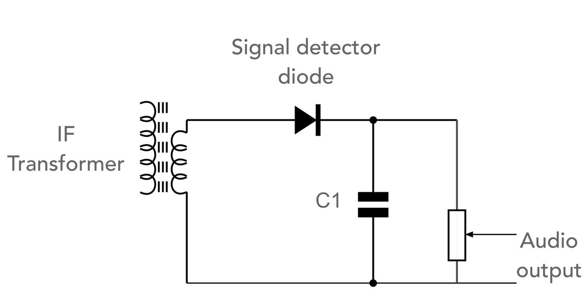
Back to Basics: The Elegant Simplicity of the AM Diode Detector In an era of complex SDRs and digital signal processing, there is something deeply satisfying about a circuit that can extract information using just three components. The AM Diode Detector (or envelope detector) remains the bedrock of radio history and a perfect case study in elegant engineering. How does it work? At its core, it’s a three-stage process of "clean and smooth": 1. Rectification: The diode acts as a gate, passing only one half of the RF signal. 2. Filtering: A capacitor charges to the peak voltage of the RF pulses, "filling in the gaps" between cycles. 3. Recovery: A resistor allows the capacitor to discharge at a rate that follows the audio envelope, but not the high-frequency carrier. The Engineering Trade-offs: While simple, it isn't perfect. Professional designs have to account for: 🔹 Turn-on Voltage: Silicon diodes (0.6V) are often too "insensitive" for weak signals, making Germanium or Schottky diodes (0.2V - 0.3V) the gold standard for these circuits. 🔹 Selective Fading: The envelope detector can struggle with distortion if the carrier signal fades relative to the sidebands. 🔹 Diagonal Clipping: If the RC time constant is too long, the output can't fall fast enough to follow the audio, leading to distortion. Whether you're building a crystal set or designing a modern RF level detector, understanding these basics is key. Check out the link in the comments. #ElectronicsEngineering #RFDesign #RadioTech #ElectricalEngineering #AnalogDesign #ElectronicsNotes
6
9
72
2,728