Filter
Exclude
Time range
-
Near
TAMPICTG87
Evaluation of Tech Industry Revaluation and Application Deployment The report’s core logic focuses on shifting the focus of tech investment from simple "model parameter stacking" to "application scenario deployment" and "full-chain industrial reconstruction." The rationale is that declining model invocation costs have lowered the threshold for application experimentation, shifting the value logic toward enterprises capable of integrating data, workflows, and payment closed-loops. Regarding quantitative metrics mentioned—such as a 133-fold increase in model invocations over 18 months and a 415-fold increase over 20 months—these are marked as 【Unverifiable】 due to the absence of complete statistical samples, time series, and comparative criteria. While model capabilities show potential to change production functions in fields like materials science (e.g., discovering 381,000 new crystal structures) and programming efficiency (e.g., a 55.8% task completion speedup), the report’s direct correlation between "model usage expansion" and "corporate profit elasticity" lacks financial data support. The revaluation of the industrial chain covers general-purpose and specialized chips, optical interconnects, storage, advanced packaging, and domestic semiconductors, with a focus on cluster interconnects and packaging yields. Public records confirm that advanced computing and semiconductor equipment are significantly impacted by export controls, making domestic substitution a matter of both policy and security. However, in deriving the valuation premium for the shift from "passive substitution" to "innovative self-reliance," the report severely lacks key financial and operational indicators such as yields, gross margins, customer certification cycles, and actual capacity realization. Furthermore, the technical description of autonomous driving as "ADS 6.0 in 2021" is 【Inconsistent with Public Records】 when compared to the existing NHTSA ADS 2.0 framework, indicating a lack of rigor in the review of technical roadmaps. The narrative of "future industries" covers humanoid robots, brain-computer interfaces, the space economy, nuclear fusion, and innovative medicine. While these have policy-driven logic, they lack financial models for commercialization tipping points. Except for the external口径 (口径) regarding innovative drug licensing transactions (approx. $137.7 billion in 2025), most forecasts are marked as 【Unverifiable】. The report exhibits a strong "fund sales" context, using concepts like "interstellar computing power" and "expeditions" to package industry uncertainty as a sense of urgency. Decision-makers should be wary of theme rotation risks brought by such macro-narratives; any "future industry" that has not undergone order penetration, cash flow realization audits, and regulatory checkpoint verification should not be priced as a deterministic growth asset. [Keywords]: #TechIndustry #RevaluationLogic #DomesticSubstitution #ApplicationDeployment #ModelInvocation #ComputingCluster #AdvancedPackaging #OpticalInterconnects #SemiconductorEquipment #HumanoidRobots #BCI #SpaceEconomy #NuclearFusion #InnovativeMedicine #ProductionFunction #ADS #ExportControls #YieldRate #GrossMargin #CapitalExpenditure #IndustrialPolicy #CommercialClosedLoop #NarrativeReconstruction #InvestmentThemes #IndustrySecurity #RiskDiscounting #SupplyChainCollaboration #IntelligentConnectedVehicles #HighLevelAutonomousDriving #IndustryCycle [Analysis/Viewpoint] This report is essentially a "map of capital imagination." Its core function is to stitch macro-policy and tech narratives together through industrial chains, thereby increasing capital's tolerance for long-cycle, high-volatility tech assets. Its true value lies not in providing tradeable entry points, but in demonstrating the shift in tech investment narratives: from focusing on "which model has the strongest computing power" to "who can embed technology into rigid workflows and form a fee-generating closed loop." This shift aligns with the laws of industrial evolution, as the value of AI is fundamentally determined by its ability to alter production functions. Expert Perspective Collision: The Radical View: Believes the tech industrial chain is undergoing its second paradigm revolution since the mobile internet era. R&D progress in fields like BCI and nuclear fusion possesses "asymmetry"; once a breakthrough occurs, current valuation models will become obsolete, justifying configuration via an "options pricing" perspective. The Neutral View: Argues that tech investment has entered a "cool-headed reflection" phase. The report conflates "policy traction" with "commercial cash flow." Without real order quality, stable gross margins, and healthy cash inflows, the so-called "industrial chain revaluation" is merely a "valuation castle in the air" built on redundant construction. The Conservative View: Contrarily points out that the report overly downplays quantity-production constraints. Improved performance in computing clusters does not equal growth in gross profit, and the security logic of domestic substitution does not equate to endogenous innovation. Many directions listed as "future industries" remain in the "subsidy-driven" balance-sheet-consumption stage, rather than the profit-conversion stage. Blind Spot Assessment: The report's biggest logical blind spot is the "compound error of macro-narratives." Each segment looks reasonable in isolation based on policy logic, but when strung together into a conclusion of "total tech revaluation," the realization probability drops geometrically due to the stacking of supply chain bottlenecks, yield constraints, and market scale assumptions. Decision Implications and Strategic Dimensions: Decision-makers must strictly distinguish between "thematic observation portfolios" and "deterministic growth assets": Verification Sequence: One must follow the logic: "First, order penetration (Are there real paying customers?), then gross profit realization (Have margins improved?), and finally, regulatory checkpoints (Are compliance boundaries clear?)." Beware of Concepts: Strategies that use non-commercialized fields like autonomous driving, humanoid robots, or fusion as valuation benchmarks must have their asset weights drastically reduced. Dynamic Game Theory: Tech industry investment should treat "policy intensity" as a volatility indicator rather than a performance-certainty indicator. Any "domestic substitution" concept unable to provide a trajectory of continuous gross margin improvement should be priced with extreme caution. This report serves as a "thematic radar" to track industry frontiers but must never be used as a singular reference for buying decisions. The valuation logic for the tech industry has changed: if technology cannot be embedded into a payment closed-loop, even the most burning narrative cannot be converted into investment Alpha.
1
70
HeddaMacDonald5
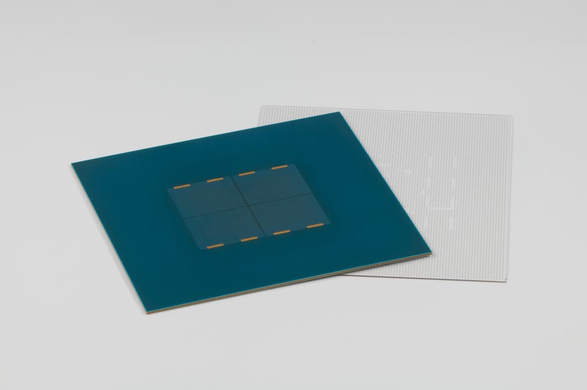
Samsung Electro-Mechanics holds a 66% stake! This glass substrate core materials joint venture is officially established...ic-pcb.com/samsung-electro-m… #SamsungElectroMechanics #GlassSubstrate #Semiconductor #AdvancedPackaging #ICSubstrate #ChipPackaging #AIInfrastructure #HPC
30
TAMPICTG87
Analysis of Technical Adjustments and Policy-Driven Sector Rotation in the A-Share Semiconductor Market On July 6, 2026, the A-share market experienced significant volatility and divergence on the first day of the implementation of new trading regulations. By the market close, the Shanghai Composite Index edged up by 0.08%, the Shenzhen Component Index fell by 0.36%, and the ChiNext Index declined by 0.51%. The STAR 50 Index, which dropped more than 3% during intraday trading, staged a recovery to close up by 1.96%. Total market turnover reached 2.21 trillion yuan, an increase of 146.5 billion yuan from the previous trading day, indicating ample liquidity. However, domestic institutional investors were net sellers, offloading 760.4 billion yuan. The market saw more stocks decline than rise, with less than half of the listed companies posting gains and a median return of -0.92%. This reflects a concentrated profit-taking move by capital in previously hot areas such as computing hardware and the chip supply chain, leading to sharp corrections in related sectors, including PCB and computing hardware concept stocks. The market hotspots exhibited a clear trend of rotation between sectors. While technology hardware stocks fluctuated, sectors such as biopharmaceuticals, banking, pork farming, and diamond heat dissipation performed strongly. The innovative drug sector led the gains, driven by policy signals, with multiple targets hitting the daily limit. Regarding market news, attention was focused on the potential delivery delays for NVIDIA’s Kyber racks due to challenges in PCB manufacturing processes. Simultaneously, the "Tao Law" V2 paper released by Huawei’s He Tingbo clarified the future evolution roadmap for advanced packaging and EDA toolchains, reinforcing long-term expectations for domestic semiconductor engineering implementation. Furthermore, the Ministry of Science and Technology emphasized promoting breakthroughs in core technologies such as integrated circuits, while the U.S. Department of Defense's initiation of a strategic lithium carbonate stockpile had marginal effects on related material sectors. From the perspective of capital logic and policy orientation, the A-share market is currently in a transition phase from "aggregate games" to "structural excavation." The selling of tech stocks by domestic institutional investors is not a rejection of industrial fundamentals, but rather a defensive reallocation in response to short-term overvaluation and shifts in after-hours liquidity brought about by the new trading rules. The semiconductor manufacturing sector’s intraday gain of approximately 3% suggests that core institutional funds remain committed to specific technical segments. Investors should note that the market is assigning a higher premium to sectors with clear industrial logic, such as advanced packaging and innovative drugs, while overcrowded tracks lacking real earnings delivery face significant profit-taking pressure in the short term. Keywords: #A-shares #STAR50 #IntegratedCircuits #HuaweiTaoLaw #InnovativeDrugs #AdvancedPackaging #EDAToolchains #PCBBottlenecks #LithiumCarbonateStockpiling #InstitutionalReallocation #NewTradingRules #IndustrialUpgrading #MinistryOfScienceAndTechnology #Liquidity #Biopharmaceuticals #ComputingHardware #IntradayDivergence #StockGame #SemiconductorManufacturing #StructuralOpportunities #ProfitTaking #ValuationCorrection #KyberRack #LowAltitudeEconomy #StrategicEmergingIndustries #SemiconductorEquipment #DiamondHeatDissipation #NMPA #MarketRotation #MarketSentiment Perspective: The trading session on July 6 serves as a microcosm of the structural adjustment and the transition between old and new rules in the A-share market. Structural Decomposition: While the indices appeared to fluctuate mildly (Shanghai Composite 0.08%), intense capital redistribution occurred beneath the surface. The decline of over 3,500 stocks alongside increased volume indicates that the market is not in a "wait-and-see" mode, but rather in a period of high-intensity "position shifting." Capital has flowed out of overcrowded sectors like computing hardware and into areas with stronger policy certainty (innovative drugs, critical IC technologies) and defensive attributes (banking, pork), aligning with the market's self-correcting logic following the implementation of new rules. Logic Review: The release of Huawei’s "Tao Law" V2 paper acts as a "stabilizing needle" for the tech core of the market. It shifts the focus from short-term PCB manufacturing bottlenecks to deeper integrated circuit technological evolution (e.g., Logic Folding, 3D Folding). This implies that the market’s assessment of the semiconductor industry is upgrading from a "capacity gap" perspective to an "engineering implementation capability" perspective. Meanwhile, the sell-off in computing hardware reflects concerns over "diminishing marginal returns on computing infrastructure," suggesting that hardware deployment alone is no longer sufficient to sustain valuation inflation. Expert Discussion: The Radical View: The slump in PCB and computing hardware is a "perfect washout," with the market utilizing the policy transition window to exchange chips, aiming to clear the way for the next wave of technology-driven momentum. The Neutral View: The market is in a passive transition phase guided by policy. Under the new rules, market volatility will be more direct. The 760 billion yuan sell-off by institutional investors indicates concerns over short-term liquidity uncertainty; focusing on defensive sectors with valuation protection, such as pharmaceuticals, is advised. The Conservative View: One must be wary of the "profit-taking trap" potentially hidden behind the 3% gain in the semiconductor manufacturing sector. Given that market volume has increased but the number of rising stocks remains limited, it is prudent to reduce exposure to high-volatility themes and focus on the strength of subsequent earnings reports in validating industrial logic. Strategic Implications: The current market does not face a "crash risk" but is instead in a stage of deep structural maneuvering. Decision-making should focus on: 1) Identifying companies with an R&D "moat" capable of overcoming manufacturing challenges; 2) Avoiding hardware tracks that rely on excessive leverage or single-theme hype; and 3) Following the guidance of the Ministry of Science and Technology and the NMPA, laying out positions in core assets with potential in both key technology and global commercialization. The market is currently screening for true growth rather than simple sector beta.
41
TAMPICTG87
Assessment of Technology Industry Revaluation and Application Implementation The technology industry is currently undergoing a paradigm shift from "competitive model parameter metrics" to "scenario integration and commercial closed-loops." The primary driver of growth has pivoted significantly toward how data, scenarios, workflows, and payment loops are effectively integrated. While the exponential growth in model API calls has indeed lowered the marginal cost of application development and experimentation, logical deductions regarding the elasticity between call volumes and profitability often fall short due to the lack of reproducible statistical scope, time-series data, and actual customer conversion rates, making it difficult to directly equate "model buzz" with "financial returns" 【Unverified】. Computing power competition has evolved intergenerationally, with the focus shifting from single-chip performance to the synergistic efficiency of cluster interconnection, memory bandwidth, advanced packaging, optical module supply, and cloud provider capital expenditures (CAPEX). Although structural opportunities for domestic substitution exist in various sub-sectors driven by policy and security mandates, the report significantly downplays critical constraints such as yield ramp-up periods, customer certification cycles, actual capacity realization, and gross margin volatility when discussing valuation markups. Current market forecasts for fields like humanoid robotics, the space economy, and controlled nuclear fusion are constrained by technical path uncertainty, with most key mass-production data and commercialization thresholds lacking unified, authoritative measurement standards 【Unverified】. The investment logic in the technology sector is converging from the "breadth of technical roadmaps" to "commercial feasibility in rigid scenarios." While policy orientation confirms the industrial security status of fields such as brain-computer interfaces, innovative pharmaceuticals, and intelligent connected vehicles, policy guidance does not equate to immediate commercial cash flow returns. The market is currently saturated with thematic narratives attempting to mitigate the uncertainty of long-term technology investment by constructing grand blueprints. If investors or decision-makers overlook real order payments, gross margin restoration, and regulatory node confirmation, they are highly susceptible to "asset misallocation traps" caused by thematic rotation. [Keywords]: #TechnologyIndustry #Revaluation #ApplicationImplementation #ComputingClusters #DomesticSubstitution #CommercialClosedLoop #IndustrySynergy #TechnicalRoadmap #ScenarioEfficiency #GenerativeModels #AdvancedPackaging #OpticalModules #HumanoidRobotics #BrainComputerInterface #SpaceEconomy #ControlledNuclearFusion #InnovativePharmaceuticals #DigitalProductivity #IndustrialPolicy #InvestmentTrap #CapacityRealization #YieldRampUp #CAPEX #IndustrialSecurity #ValuationDeviation #TechnicalParameters #MassProductionConstraints #ScenarioIntegration #InvestmentCycle #MarketCapacity Key Takeaways The credibility of this report falls into the range of "comprehensive industry mapping but broken valuation logic." Its core value lies in constructing a panoramic "imagination map" that links computing power, hardware, applications, and future sectors, effectively sorting out the complex connections in the technology industry from underlying infrastructure to end-user terminals. However, as an investment model, it suffers from a clear case of "narrative over evidence." Equating the "inevitability of technical progress" with the "certainty of commercial investment" is a common composite error in such tech narrative reports: individual arguments for each segment may hold technical merit, but when strung together into an investment conclusion for the entire chain, the probability of realization drops geometrically. From a non-traditional perspective, the essence of tech investment has long shifted from "discovering the strongest model" to "finding real customers with a willingness to pay." The report correctly captures the improvement in production functions through AI in engineering R&D (such as crystal structure discovery) and commercial efficiency, but this precisely highlights the capital market's over-preference for "grand narratives"—ignoring engineering bottom lines such as mass-production constraints, yield bottlenecks, post-sales liability, and safety certification, which are the true determinants of net profit margins. Blind Spot Warnings: Capacity Illusion: The report treats the urgency of domestic substitution as a direct driver for valuation premiums, yet fails to disclose the yield ramp-up periods, the surge in upfront R&D investment, and the gross margin gap compared to international competitors during the localization process. Policy Lag Risk: Confusing policy orientation with commercial cash flow ignores the risks of subsidy dependence, overcapacity due to redundant construction, and the iterations and friction inherent in standard-setting processes. Composite Narrative Error: Forcibly integrating vastly different fields like humanoid robotics and nuclear fusion makes it easy to induce investors into making erroneous asset pricing comparisons across different technical cycles and commercialization stages. Decision-Making Implications: Prioritize Verification Logic: When facing such "full-chain revaluation" views, establish a four-tier verification sequence: "Orders—Gross Margin—Cash Flow—Regulation." Assess order quality and actual payment first, then verify compliance with policy security boundaries. Downscale Narrative Usage: Treat this report as an "industry radar" rather than a "buy guide." Use the covered industry chain segments to inspect your own supply chain layout or investment depth, but strictly forbid the use of growth rates and valuation multiples within the report for financial modeling. Hedge Against FOMO: Tech investment often triggers anxiety caused by "thematic rotation." Maintain immunity to "narrative urgency" by examining long-cycle inventory fluctuations and CAPEX cycles, returning to independent judgments on product strength and commercial landing capabilities. Summary: This report is a popular science guide to understanding the tech investment landscape, not a quantitative tool for asset pricing. For participants in the tech industry, the focus should shift from "how grand the narrative is" back to "how stable the product delivery is."
1
121
antfeedapp
THE AI SERVER COMPONENT MAP: SAMSUNG ELECTRO-MECHANICS PUTS $15B INTO FC-BGA AND MLCC TLDR: Samsung Electro-Mechanics is turning Busan and Sejong into Korea’s AI server component base. The company will invest ₩23 trillion ($15 billion) by 2040 to expand FC-BGA package substrates and high-value MLCC capacity. Busan gets the larger piece: ₩15 trillion ($9.8 billion) by 2040 to build core production lines for high-value MLCCs and expand advanced package substrates including FC-BGA. Sejong gets ₩8 trillion ($5.2 billion) to become a global manufacturing hub for AI server package substrates, with investment in production equipment and R&D. The split is clear. Busan becomes the high-value MLCC base, while Sejong becomes the FC-BGA and advanced package substrate hub for AI servers. Samsung Electro-Mechanics is also expanding overseas. It will invest ₩1.8 trillion ($1.2 billion) in Vietnam to increase FC-BGA capacity, while its Philippines site received ₩75 billion ($49 million) last year to respond to rising MLCC demand. Samsung’s AI supply-chain buildout is moving below the chip itself: package substrates, MLCCs, production lines, R&D and regional manufacturing hubs. #SamsungElectroMechanics #삼성전기 #Samsung #삼성 #FCBGA #MLCC #PackageSubstrates #패키지기판 #AIServers #AI서버 #AdvancedPackaging #첨단패키징 #Busan #부산 #Sejong #세종 #Semiconductors #반도체 #Korea #한국 $SSNLF $SOXX $SMH $EWY $KORU
1
263
antfeedapp
PACKAGING CHEMICALS: LG CHEM WINS AMKOR STRIPPER SUPPLY DEAL TLDR: LG Chem is moving from display chemicals into advanced semiconductor materials, using Amkor as its first major OSAT validation point as AI and HBM push packaging quality higher. LG Chem will mass-supply a customized photoresist stripper to Amkor’s new production line, cutting residue-removal time by about 50% versus the existing process. The win expands LG Chem’s chip-packaging materials push across CCL, DAF and PID. #LGChem #Amkor #SemiconductorMaterials #PhotoresistStripper #AdvancedPackaging #OSAT #HBM #ArtificialIntelligence #ChipPackaging #Semiconductors #MemorySemiconductors #SouthKorea
3
2
119
TAMPICTG87
Insights into IC Talent Supply-Demand and Job Structure The integrated circuit (IC) industry is currently navigating a cycle of deep misalignment between talent demand structures and skill supply. Data shows that in 2025, the volume of job postings on the platform increased by 5.10% year-on-year, with an average offered annual salary of approximately 256,100 RMB, an increase of 8.08%. Job profiles demonstrate a distinct trend toward "higher educational requirements and complexity": demand for master's degree holders rose by 32.7%, while mature talent with 3–5 years of experience remains the market mainstay; demand for senior talent with 5–10 years of experience grew by 16.0%. Although the global market growth forecast aligns with industry consensus, key indicators such as the local market size and industry self-sufficiency rate deviate from authoritative sales data due to discrepancies in statistical definitions 【Inconsistent Sources】. Recruitment priorities have shifted from simple chip design to cross-disciplinary composite roles, including overseas sales, supply chain procurement, automotive engineering, and compiler development. Talent distribution exhibits a high degree of regional concentration, resulting in job demand densities within tier-one IC industrial clusters that far exceed the current size of the accessible talent pool. There is a significant lag between enterprise-side expansion demands and the supply speed of visible talent on the platform. While undergraduate degree holders account for nearly half of the structure, the proportion of PhD holders is only about 1.06%, highlighting a structural gap between the current talent age/education composition and the industry's transition toward advanced packaging and leading-edge process nodes. Job rankings reveal that market hotspots have shifted from traditional algorithm engineering toward critical nodes—such as verification, process integration, simulation, and optical design—within scenarios like "global expansion, automotive applications, and domestic supply chain substitution," reflecting the urgency enterprises face regarding technical bottlenecks and supply chain restructuring. Current recruitment intensity in the industry somewhat masks deeper issues in organizational capability allocation. Enterprises are not merely lacking junior developers; they are acutely deficient in core, mid-to-senior level talent capable of taking direct ownership of complex projects, achieving cross-stack collaboration, and withstanding the high uncertainty of domestic substitution. Although the premium characteristics of roles related to algorithms and system-on-chip (SoC) are significant, the salary growth rates for these roles lack unified quantile definitions and rigorous sample specifications, easily leading to the misinterpretation of recruitment premium indicators. Since recruitment heat often lags behind capital expenditure and R&D order expectations, there exists a notable risk of contraction in job demand and salary growth should downstream capacity utilization or the financing environment fluctuate. [Keywords]: #ICTalent #CompositeSkillGap #DomesticSubstitution #ChipDesign #AdvancedPackaging #AutomotiveChips #SupplyChainRestructuring #TalentProfiling #RecruitmentHeat #SemiconductorSales #IndustrySalaryPremium #AlgorithmEngineer #VerificationEngineering #OpticalDesign #ProcessIntegration #EDAtools #SoftwareDefinedHardware #TapeOut #ProjectExperience #HighEndChips #TalentReserves #OrganizationalCapabilityAllocation #IndustrialClusters #TalentSupplyDemandMismatch #JobStructuring #SemiconductorSales #ProjectDelivery #VerificationEngineer #AdvancedPackagingSimulation #TechnologyGoGlobal Key Takeaways The core value of this report lies in its function as an "industry talent thermometer" rather than a quantitative manual of industrial truth. Its most significant insight is the realization that the core control point of industrial development has shifted from early-stage "capital financing" and "broad-net hiring" to "talent efficiency realization." The essence of the talent gap is a failure in organizational capability allocation: true productive capacity can only be unlocked by those who can attract talent in "back-end and hard-core nodes," such as process integration, verification, equipment maintenance, packaging simulation, supply chain quality systems, and overseas customer support. However, the report has clear boundaries of credibility. First, it is based on a closed sample pool, omitting the vast "hidden" labor market—including campus recruitment, internal transfers, and front-line technicians at wafer fabs—leading to statistical biases in talent structure inference. Second, references to key financial and statistical categories (such as sales and import volume) are 【Inconsistent with public data】 from customs authorities and authoritative industry standards. For decision-makers, "job growth rates" should be viewed as a signal of corporate expansionary impulse rather than an indicator of robust commercial quality. Increased recruitment can sometimes stem from project delays, high turnover rates, organizational inefficiencies, or repetitive work caused by supply chain substitution pressures. Decision-Making Implications: For Enterprises: Shift focus from "broad-net hiring" to "critical profile construction internal development joint training with suppliers," particularly filling gaps in verification, process integration, packaging simulation, quality assurance, and domestic supply chain management. For Individual Developers: Avoid blindly chasing popular buzzwords; focus on building skill combinations into deliverable project evidence (e.g., tape-out yield improvement, automotive-grade certification, complex SoC verification). For Investors: Be wary of equating "recruitment heat" with "profit certainty." It is essential to scrutinize whether a company's talent allocation forms a positive reinforcement loop with technical yield, delivery capabilities, and customer adoption. Summary: This report serves as a directional clue for the talent market but should strictly NOT be used for salary negotiation decisions or investment valuation without secondary validation against a company's actual order delivery cycles and yield improvement data.
104
antfeedapp
THIS WEEK IN SAMSUNG FOUNDRY THE ANTHROPIC FOUNDRY OPENING: SAMSUNG EYES A 2NM AI LOGIC CUSTOMER TLDR: Samsung’s foundry rebound may have a new candidate. Anthropic is reportedly discussing custom AI chip production with Samsung, including possible use of Samsung’s 2nm process and advanced packaging, though the project is still at an early stage. Anthropic has reportedly started early work on its own AI chip and is expanding its chip engineering team, including hires from OpenAI’s early custom-chip group. For Samsung, the timing matters. Earlier custom AI chip development with OpenAI and Meta has reportedly stalled, leaving Samsung still searching for a large AI logic customer to prove its advanced foundry comeback. The relationship is already there. Samsung joined Anthropic’s $65 billion Series H round in May as a strategic infrastructure partner, alongside SK Hynix and Micron. At the time, Anthropic listed cooperation beyond memory and storage, including logic chips. That line now looks more important. If Anthropic moves forward, Samsung could supply the manufacturing side while Anthropic keeps using a multi-vendor compute stack across AWS Trainium, Google TPU, Nvidia GPUs, Microsoft AI chips and possibly Fractile. #Samsung #삼성전자 #Anthropic #Claude #AIChips #AI반도체 #Foundry #파운드리 #2nm #AdvancedPackaging #첨단패키징 #Nvidia #TSMC #Broadcom #OpenAI #Meta #Semiconductors #반도체 $SSNLF $NVDA $TSM $AVGO $META $GOOGL $AMZN $MSFT $SOXX $SMH
190
antfeedapp
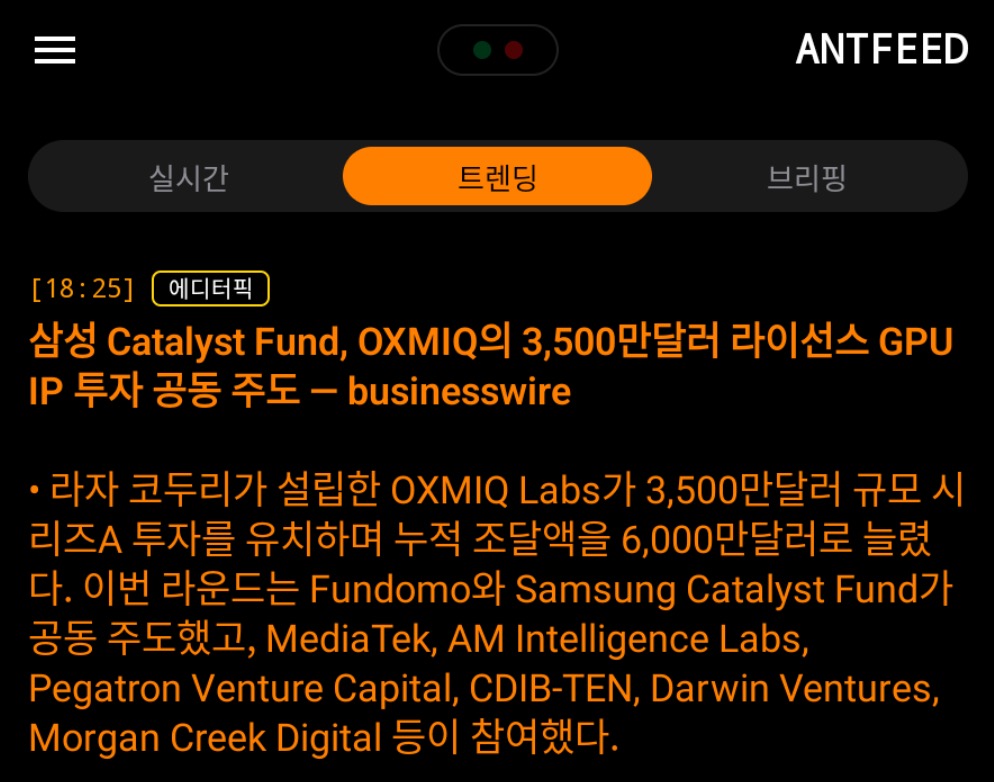
SAMSUNG’S AI IP BET: OXMIQ RAISES $35M TO SCALE LICENSABLE GPU ARCHITECTURE TLDR: Samsung is backing a different kind of AI chip play: not another full-stack GPU challenger, but a configurable GPU IP layer that lets more companies build custom AI silicon without owning the entire chip roadmap. OXMIQ, founded by Raja Koduri, raised a $35 million Series A co-led by Samsung Catalyst Fund and Fundomo, bringing total funding to $60 million. Its OxCore architecture combines a CUDA-compatible GPU engine, tensor engine and orchestration engine, while OxQuilt lets customers design across foundries, memory types and packaging options. #SamsungElectronics #SamsungCatalystFund #OXMIQ #RajaKoduri #Fundomo #MediaTek #Pegatron #IntelCapital #Tenstorrent #JimKeller #ArtificialIntelligence #GPUArchitecture #CustomSilicon #SemiconductorIP #Chiplets #NearMemoryCompute #AdvancedPackaging #AIInfrastructure #AIChips
56
TAMPICTG87
Evaluation of the New Semiconductor Paradigm under "Time-Scale Micro-Narratives" The report posits a fundamental shift in semiconductor evolution: moving the primary metric of advancement from "gate width/area" to "latency/system efficiency." It argues that as geometric scaling hits limits imposed by quantum tunneling, interconnect RC delays, power density walls, and skyrocketing capital costs, the industry must prioritize reducing the "end-to-end time constant" (τ=R×C). 1. Core Claims and Verification Status Industry Context: The report's themes were presented at ISCAS 2026 (May 24–27, 2026). The entity behind these claims reports the mass production of 381 chip designs over the past six years. Projections: It claims the 2026 autumn Kirin chips will employ "logic folding" (logical stacking) and that by 2031, advanced chip density will reach the equivalent of 1.4nm process nodes. Verification Gaps: Specific performance metrics—such as 238 MTr/mm², P-core power efficiency 41%, 3.1GHz/5.0GHz clock speeds, and the "Mate 90" reference—are not present in public releases and are marked as "unverifiable." Economic Arguments: The report asserts that the "old paradigm" (scaling via EUV/Advanced Nodes) is bankrupt due to costs (e.g., $20B per 3nm/2nm fab, $400M per High-NA EUV machine). These figures are industry estimates rather than verified internal costs and are treated as strong推断 (strong inferences) rather than confirmed facts. 2. Strategic Shift: "Time Constant" vs. "Node Worship" The report advocates for a narrative framework that unifies circuit time constants, interconnect delays, data movement, compilation scheduling, and system interconnection. The "τ Strategy": Even if advanced nodes are physically constrained, performance/efficiency gains can still be pursued through 3D layout, packaging interconnects, protocol unification, and hardware-software co-optimization. Systemic Blind Spots: The report interprets rising advanced node costs as the "failure of the old paradigm." However, high costs do not equate to the disappearance of demand. AI, High-Performance Computing (HPC), and High-Bandwidth Memory (HBM) continue to drive demand for the most advanced equipment available. Analysis and Perspective The real value of this report is not in "proving" that advanced lithography (EUV) is being replaced, but in establishing a Systemic Latency Governance framework. Parallelism vs. Substitution: If the "τ strategy" proves successful, it will likely function as a parallel performance booster for existing architectures, not a total replacement for EUV, GAA (Gate-All-Around), or Backside Power Delivery. The "Missing Link": The report lacks critical data points required for commercial verification, such as test workloads, benchmark chips, manufacturing yields, thermal density profiles, and actual manufacturability data. Without these, it serves as a strategic hypothesis rather than a completed industry fact. Strategic Recommendations For Industry Research: Track the following technologies as primary indicators of the "τ" paradigm: Logic Folding (Logical stacking/folding) Unified Bus/Optical Interconnects Chiplet Architectures & Advanced Packaging EDA and Compiler Co-optimization For Investment Due Diligence: Separate the report’s variables into three distinct buckets: Verified Events: Published roadmaps and announced product releases. Engineering Hypotheses: Metrics like "equivalent 1.4nm density" that require proof of manufacturability and thermal stability. Commercial Extrapolations: Market trends (e.g., the decline of High-NA EUV demand) that are largely speculative. Investment Caution: Avoid mapping "domestic substitution sentiment" directly onto the "decline of the equipment supply chain." The equipment chain (EUV/Advanced Foundry) remains the absorption layer for high-end compute demand. The shift to a "τ-centric" model is a complex transition, not a sudden market replacement. Conclusion: The report is a significant conceptual shift from "process node worship" to "system latency governance." While its technical vision is compelling for engineers, it requires rigorous validation of yield, power, frequency, and cost data before being used as a basis for high-stakes capital allocation or industrial pricing models. Keywords #SemiconductorParadigm #τStrategy #LatencyGovernance #ISCAS2026 #KirinChip #LogicFolding #AdvancedPackaging #Chiplet #SystemEfficiency #HighNAEUV #ProcessNodes #ThermalDensity #HardwareSoftwareCoDesign #EDA #CompilerOptimization #EUV #GAA #BacksidePowerDelivery #ComputationalEfficiency #SupplyChainDynamics
97
RaymingTech
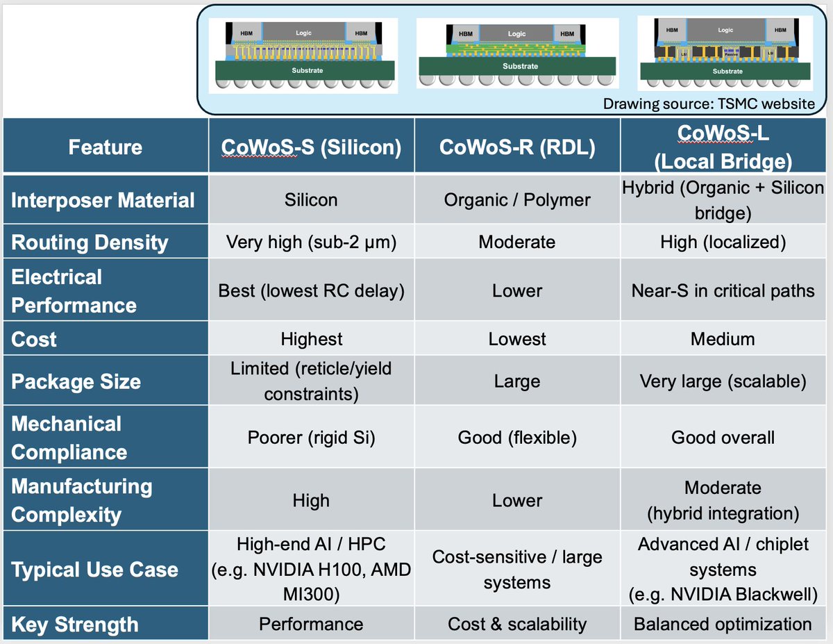
GPUs used to sit on PCBs next to GDDR memory, talking to each other through long board traces. That worked — until it didn't. Long interconnects meant high RC delay, limited I/O density, lower bandwidth, and more energy burned per bit. As AI workloads scaled, the architecture hit a wall. The industry's answer: heterogeneous integration — pulling logic and memory into a single package. TSMC's Chip-on-Wafer-on-Substrate (CoWoS) is one of the most important enablers of this shift. The idea is straightforward: place the GPU and HBM side-by-side, connect them through a fine-pitch interposer, and eliminate the long PCB traces that were killing performance. The interposer is the key piece here. It's a high-density wiring layer that enables short die-to-die connections, fine-pitch routing, and bridges chip I/O to the package. Two main flavors exist — silicon (precise, expensive) and organic RDL (cheaper, larger area). CoWoS comes in three variants, each making a different tradeoff: CoWoS-S uses a silicon interposer with ~0.5–2 µm routing. Maximum density and performance, but limited by reticle size and cost. CoWoS-R uses an organic RDL substrate. Lower cost, larger footprint, more flexibility — with some density tradeoff. CoWoS-L combines an organic base with localized silicon bridges only where high density matters most (think: GPU-to-HBM interface). It's the architecture showing up in large-scale AI systems because it balances performance, cost, and scalability. The bottom line: CoWoS replaces long PCB interconnects with fine-pitch packaging — and that shift is a big part of why modern AI accelerators can deliver the bandwidth they do. (Comparison table in the comments.) #Semiconductors #AdvancedPackaging #CoWoS #HeterogeneousIntegration #Chiplets #AIHardware #HPC #TSMC #HBM #ElectronicsEngineering
5
357
CNBCTV18News
"Without advanced packaging, there is no AI." 🧠💾 Everyone is talking about AI chips, but the real secret to their power isn't just making them smaller—it's how we pack them together. Audrey Charles (SVP, Advanced Packaging & President, Lam Capital) joins Voices From The Valley to break down why advanced packaging is the true unsung hero of the AI revolution, driving energy efficiency and deep-tech innovation. Watch the full episode: youtu.be/A56lVVK5OPc @ShereenBhan #AIChips #Semiconductors #DeepTech #AdvancedPackaging
2
6
7,175
the_analyst_24
The AI packaging bottleneck just found a dual-engine accelerator in Japan, and the market is completely mispricing the structural velocity here. Following last month's breakthrough, Polish deep-tech pioneer XTPL S.A. $XTP.WA has just secured its second massive independent contract in the hyper-demanding Japanese semiconductor ecosystem. This isn't a fluke—it is definitive proof of institutional commercial replicability in the world’s most stringent quality-control market. Here is the institutional breakdown of why today's news radically de-risks the long-term semiconductor thesis: 1/ THE CATALYST: REPLICATED JAPANESE ADOPTION XTPL will deliver its Delta Printing System (DPS) alongside a custom laser sintering system to a major, multi-decade Japanese manufacturer of automated industrial equipment. Crucially, this is an entirely separate partner and project from the Ultra-Precise Dispensing (UPD) module sale announced in June. The hardware is slated for delivery in H2 2026, targeting advanced yield management for high-density interconnects (HDI/UHDI) and semiconductor substrates. 2/ UNDERSTANDING THE PIPELINE: STAGE 3 VS. STAGE 4 To appreciate the revenue visibility, you have to look at XTPL’s strict 5-stage industrial deployment framework. • June’s deal was a Stage 4 milestone (integrating a UPD module into a client's prototype industrial machine for pilot lines). • Today’s deal officially advances this new partner to Stage 3 (independent laboratory validation via the DPS device). The fact that two independent Japanese Tier-1 giants are concurrently moving down the commercial pipeline for the exact same strategic application—high-precision dispensing of native copper conductive paths—confirms that the semiconductor industry is aggressively hunting for XTPL's specific physical solution. 3/ THE HARDWARE MOAT & THE AI PACKAGING CRUNCH Advanced packaging (CoWoS, high-density substrates) remains the ultimate physical choke point of the global AI supercycle. Yield management is where billions of dollars are won or lost. XTPL's proprietary UPD technology solves this by printing sub-micron conductive traces (1–100 μm) on complex 3D surfaces without nozzle clogging. The razor-and-blade moat here is pristine. This process relies on a tight interdependency between XTPL’s precise nozzle geometry and their proprietary nanoinks (specifically the upcoming copper formulation). You cannot reverse-engineer the hardware without utilizing their consumables, creating an exceptionally high-barrier, high-margin recurring revenue stream once fully integrated. 4/ ASYMMETRIC UP-SIDE & THE CFO’S HINT The macro narrative has been overly fixated on near-term technicalities, specifically the PLN 15–20M capital gap in H1 2026 to scale their High-Mix Low-Volume (HMLV) production line. This dilution anxiety is creating an incredible entry window. Management is targeting PLN 100M in commercial sales by 2028, scaling to PLN 150M by 2030. With hardware and consumables yielding projected 35-40% margins at scale, a standard 12x-15x EV/EBITDA multiple implies a 2030 Enterprise Value of PLN 720M - 900M—representing a realistic 4x to 5x upside from current levels. Furthermore, CFO Jacek Olszański explicitly noted today that if this new Japanese project achieves full industrial deployment, its commercial potential is significantly larger than the breakthrough Chinese deployment that has been scaling since January 2025. THE BOTTOM LINE XTPL is transitioning from a speculative deep-tech bet into a highly validated, institutional-grade semi cap play. At current valuations, the market is discounting their absolute grip on precise photonic interconnects, making them a premier, bite-sized M&A target for semiconductor infrastructure consolidators like Applied Materials, ASML, or Nano Dimension. For investors looking for pure-play alpha in the physical layer of AI infrastructure, XTPL remains an elite micro-cap "pick and shovel." Disclaimer: Not a financial advice. Always do your own DD. #XTPL #Semiconductors #AdvancedPackaging #AI #MicroCap #DeepTech #Investing #TechStocks tradingview.com/news/eqs:4f2…
Deep-Dive Equity Research: The Hidden Micro-Cap Bottleneck in AI & Advanced Packaging Today, we are tearing down XTPL S.A. ($XTP.WA) – a deep-tech company solving a massive physical constraint in next-gen microelectronics. Here is the complete investment thesis on this Polish tech innovator: 1. Company Overview 🔹 Company: XTPL S.A., based in Wroclaw, Poland, is a global deep-tech company developing breakthrough ultra-precise printing technologies for nanomaterials. 🔹 Shareholders: High free float with strong management skin-in-the-game (CEO Filip Granek). Currently assessing strategic investors or a share issue to bridge a PLN 15–20M capital gap in H1 2026. 🔹 Past to Future: Transitioned from pure R&D prototyping to full commercialization. While the PLN 100M revenue target was shifted from 2026 to 2028, they are now executing their first industrial implementations with tier-1 global manufacturers. 🔹 Technology: The moat is their proprietary Ultra-Precise Dispensing (UPD) technology. They can print conductive traces (like native copper) down to 1–100 μm on complex 3D surfaces. This is critical for advanced packaging, Photonic Integrated Circuits (PICs) for AI data centers, and FPD open defect repair. 2. Product & Current DevelopmentsXTPL operates a highly lucrative "razor-and-blade" model: ⚙️ UPD Modules: Industrial printheads integrated directly into the production lines of global electronics manufacturers. 🔬 DPS (Delta Printing System): Laboratory prototyping devices. 🚀 The Game-Changer (ODRA System): Launched in March 2026, ODRA is designed for High-Mix Low-Volume (HMLV) industrial production. They just secured their first Silicon Valley client (advanced packaging/defense) for ~$400k-$500k per unit (over 2x the price of DPS). 🧪 High-Performance Materials (HPM): Proprietary nanoinks (e.g., new copper inks launching H2 2026) that create recurring, high-margin revenue. 3. Technology Moat, Patents & Product Interdependency The core investment thesis rests on an ironclad intellectual property (IP) fortress and deep technological interdependency. XTPL does not just sell a machine; they own a proprietary ecosystem protected by a growing global patent portfolio spanning over 26 patent families and dozens of granted patents worldwide (covering the US, Europe, China, Japan, and South Korea). This deep IP moat covers three highly interdependent pillars: 🧪 The Ink Formulation: Highly concentrated metallic nanoparticles (silver, gold, and the upcoming copper) with precise rheological properties. 📐 The Nozzle Geometry: Ultra-precise inner diameters designed to resist clogging while allowing continuous extrusion. ⚡ The Printing Process: Software-driven hydrodynamic forces that pull the material out via high-aspect-ratio deposition rather than standard gravity-fed inkjet methods. This creates a powerful "lock-in" effect. Competitors cannot easily copy the hardware because the printheads require XTPL’s exact nanoink chemistry to function without clogging, and third-party inks ruin the sub-micron accuracy. For tier-1 industrial clients, swapping out an integrated XTPL UPD module would mean re-engineering entire multi-million dollar semiconductor packaging lines. This tech dependency forms an almost impenetrable barrier to entry. 4. Valuation Snapshot Market Cap: ~PLN 168.7M (approx. $42M USD) at ~PLN 59/share. Enterprise Value (EV): ~PLN 166.9M. Net Debt: ~PLN 10.4M (Cash: PLN 6.6M, Debt: ~PLN 17M, strictly ex-leases). EBITDA (FY2025): PLN -18M. 5. Earnings Snapshot (FY2025/Q1 2026) Revenues hit a record PLN 13.7M ( 11% YoY) from products/services, with total income (incl. grants) around PLN 15.6M. However, heavy R&D and scaling costs resulted in an EBITDA of PLN -18M and a net loss of PLN -23.3M. Cash reserves dropped to PLN 6.6M, triggering the current PLN 15-20M capital raise process to fund the aggressive scale-up of the ODRA line. 6. Peer Group Comparison XTPL competes in a niche but highly valuable space against players like Nano Dimension, Voxel8, and ioTech. Unlike Nano Dimension (which is heavily capitalized but struggles with organic growth), XTPL's tech is already being adopted by tier-1 display and semiconductor manufacturers. XTPL trades at a steep discount relative to the TAM they are attacking, largely due to their current cash burn and micro-cap status on the WSE. 7. Forecast 2030 & EV/EBITDA Valuation Management targets PLN 100M in commercial sales by 2028. Projecting into 2030, assuming successful adoption of ODRA and recurring ink sales, revenues could realistically scale to PLN 150M . With hardware/consumable hybrid models generating 35-40% margins at scale, 2030 EBITDA could reach ~PLN 60M. Applying a conservative 12x-15x EV/EBITDA multiple (standard for high-growth semiconductor equipment), the implied 2030 EV sits at PLN 720M - 900M. That represents a 4x to 5x upside from current levels, assuming they navigate the near-term dilution. 8. M&A / Takeover Fantasy Advanced packaging is the defining bottleneck for AI chips (just look at TSMC's CoWoS capacity). XTPL's ability to precisely dispense interconnects for photonics and chiplets makes them a prime acquisition target. Semiconductor equipment giants (Applied Materials, ASML, KLA) or additive manufacturing consolidators (Nano Dimension) could easily acquire XTPL for a massive premium simply to own the UPD IP. 9. Chances & Risks 🟢 Chances: Massive AI hardware tailwinds; the shift to advanced packaging and photonic circuits; validation by Silicon Valley defense and top-tier Asian display manufacturers; high-margin recurring revenue from nanoinks. 🔴 Risks: High cash burn. The immediate need to raise PLN 15-20M in H1 2026 means impending dilution for current shareholders via a share issue. Execution risk remains high as they transition from R&D to HMLV production. 10. Conclusion XTPL is a high-risk, asymmetric-reward play on the physical bottlenecks of the AI supercycle. The market is pricing in the dilution risk and cash burn, completely ignoring the strategic value of their UPD tech and the recent Silicon Valley validation of the ODRA system. If you believe that advanced packaging and hardware constraints are the real AI alpha, XTPL is the ultimate micro-cap "pick and shovel." Disclaimer: Not a financial advice. Always do your own DD. #XTPL #Semiconductors #AdvancedPackaging #AI #MicroCap #DeepTech #Investing #TechStocks
1
465
antfeedapp
WHAT MATTERED THIS WEEK THE GLASS SUBSTRATE JV: SAMSUNG ELECTRO-MECHANICS TEAMS UP WITH JAPAN SUMITOMO TLDR: Samsung Electro-Mechanics will form a glass substrate JV with Japan’s Sumitomo Chemical affiliate Dongwoo Fine-Chem, with both sides putting in about ₩480 billion ($314 million). The new JV will be called Glassem. Samsung Electro-Mechanics will own 66%, while Dongwoo Fine-Chem will own 34%. Production will be based at Dongwoo Fine-Chem’s site in Pyeongtaek, Korea, with the legal entity expected to launch before year-end. The strategic goal is glass core supply. Samsung Electro-Mechanics wants a stable glass substrate supply chain before the market becomes more crowded. Glass substrates are being watched as a potential game changer for AI semiconductor packaging, because advanced chips increasingly need better signal performance, dimensional stability and higher-density packaging. #SamsungElectroMechanics #삼성전기 #Samsung #삼성 #SumitomoChemical #스미토모화학 #DongwooFineChem #동우화인켐 #GlassSubstrate #유리기판 #AdvancedPackaging #첨단패키징 #AIChips #AI반도체 #Semiconductors #반도체 #Korea #한국 $SSNLF $SOXX $SMH $EWY $KORU #Corning #코닝
1
255
Maryli8868
SEMIXICON for Ultra-Thin Semiconductor Dicing Face Runout:≤ 2 μm Radial Runout:≤ 3 μm Vibration Intensity:≤ 0.4 mm/s semixicon.com #OpticalGlassProcessing #SemiconductorEquipment #CompoundSemiconductors #GaN #MEMSManufacturing #AdvancedPackaging #PrecisionMachining
2
TRClab2026_wiiw
$NVMI nova Ltd's WMC platform has been selected by a leading global foundry as tool-of-record for advanced packaging measurement. That means Nova did not just win an order. It won a place inside the customer’s manufacturing process. Once a tool becomes part of the production recipe, replacing it is slow, risky, and expensive. AI chips are getting harder to build. HBM. Advanced packaging. Warpage. Non-symmetric shapes. Nanometer-level measurement. The more complex chips become, the more valuable precision becomes. $NVMI Nova already controls roughly 25% of the critical dimension and film metrology market. Its tools are selected early in chip development, embedded into fabs, and protected by high switching costs. This WMC win reinforces the thesis, as AI drives more advanced packaging and HBM demand, chipmakers need more measurement intensity. Nova sells that measurement. That is why Nova remains one of the quiet toll collectors of the AI infrastructure boom. Read the full Nova research here: therationalcapitalist.substa… #Nova #NVMI #Semiconductors #AdvancedPackaging #HBM
59
Quinnsmedia1
Samsung Electronics's $90B investment is about much more than expanding production. The headline is the size of the investment. The real story is where Samsung is placing that money. From HBM memory and advanced packaging to OLED displays and next-generation batteries, Samsung is strengthening nearly every part of the AI hardware ecosystem in South Korea. That feels like a long-term strategy, not just a capacity expansion. Here's what stood out to me: • $90 billion invested across Samsung's key businesses. • Five new HBM production lines to support growing AI demand. • 250,000 new jobs that will strengthen South Korea's semiconductor talent pipeline. As AI adoption accelerates, success won't depend on who builds the biggest fab. It will depend on who can connect memory, packaging, displays, and advanced manufacturing into one resilient ecosystem. That's exactly what Samsung appears to be building. Do you think the next leader in semiconductors will be the company with the best chips, or the one with the strongest end-to-end AI supply chain? #Semiconductor #AI #HBM #SupplyChain #AdvancedPackaging #Samsung #Manufacturing #OLED #SouthKorea #Innovation
1
1
84
vaibhavparulkar
3/ Additionally, Samsung Electro-Mechanics will spend 8T won ($5.1B) to produce advanced packaging materials for AI servers in Sejong. Substrates and polymers are the hidden, yield-determining layer of advanced 3D packaging. @ASML_News #AdvancedPackaging
1
24