advisor @thru_xyz.

Joined June 2017
1,050 Photos and videos
Pinned Post
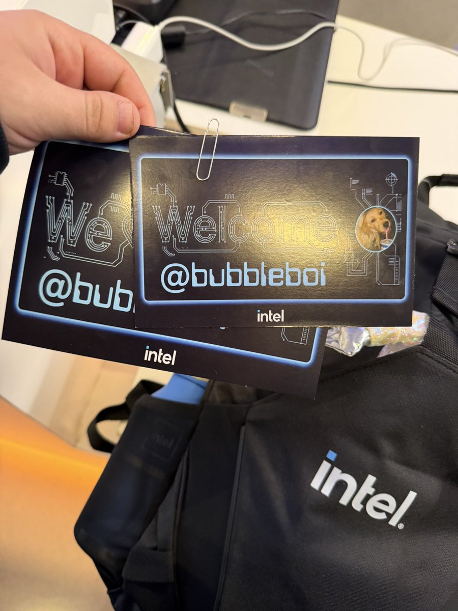
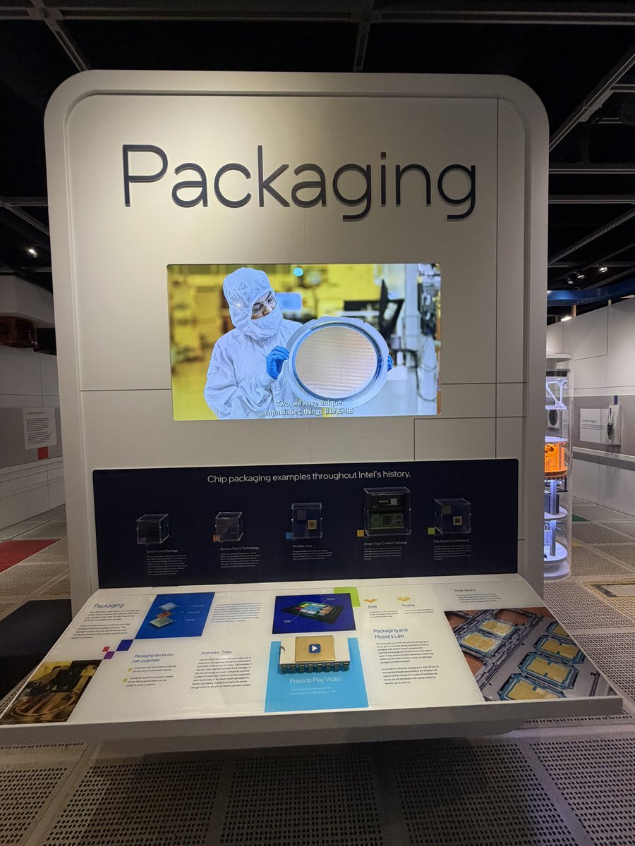
I could not put into words how much today has meant to me. I’ve been following Intel ever since I was a child and it is not an exaggeration to say they are the reason I fell in love with chips and computers in the first place. I wouldn’t have been able to take the path I have chosen in life if it wasn’t for the thousands of brilliant hard working engineers at Intel who laid the foundation for the ground I walk on. When I started following their bold bet on becoming a world class cutting edge foundry about a year ago I was galvanized by the vision that they set out. It wasn’t just important to me that Intel succeeded it was important to me that America succeeded. Silicon Valley was built by them and their cohort and it was critical to me that we not only maintained our standing in the semiconductor industry but for us to grow our industry so 100k other flowers could blossom. There was no way this could be done without an American foundry on the leading edge. I believed in the plan from the start, and as an engineer myself I was absolutely confident that Intel was developing some of the world’s greatest technology and IP from 18A to backside power delivery to the amazing breakthroughs they’ve achieved in advanced packaging which I like to dub as the new Moore’s Law. They are just getting started and there is without a shadow of a doubt more to come. Today I was vindicated for everything I’ve been talking about for over a year now. The semiconductor industry is won by those not who focus on optimizing margins but those who invest in innovation to bring value to the whole world. Lip Bu Tan and the whole Intel team have delivered on innovation… and again this is just the beginning. I will be here waiting, watching, cheering every step of the way. Thank you from the bottom of my heart for the experience, the gifts, and your words of appreciation they mean more to me that you can possibly imagine. With love, Bubble Boi 🫧♥️
60
74
1,439
451,303
“Normalize it however you want, since bandwidth is what sets throughput I bring ~190 GB per TB/s, HBM brings 24. That ratio holds whether you count chips, trays, or racks.” 😭😭😭😭😭😭😭😭
Replying to @itsclivetime
Definitely not full mesh over 576 chips my fault for glossing over that Clive. The model is an 8 chip pod, 7 ports per chip, full mesh inside the pod. Between pods you’d want a different topology, probably a torus or dragonfly, but the point I’m making is that the latency critical TP domain stays inside the pod where there are zero switch hops. Now on high batch workloads you are right past Batch 64 the MAC array throttles but since we have floorplan to spare, my simple answer is just to add more MACs 🤣🫨😎♟️✨😵‍💫 In fairness I wrote this on the toilet and my legs were going numb so I had to rush through a few details. But I want to point out also that your high batching cuts the other way as well as it drags KV with it. At B=256 with just a totally unserious 8K context that’s ~2M cached tokens or ~336 GB of KV at FP8. Reading that once per step is 42 ms at 8 TB/s, or roughly 3x the latency of GEMM. And attention itself runs at ~8 FLOPs/byte with GQA so at this high batch workload you are memory bound on basically every chip ever built, including mine. The workload you’re describing isn’t compute bound at all at real context windows 🪟 its bandwidth and more IMPORTANTLY capacity bound ! So you do the math again: per 8 TB/s of bandwidth, one 8-chip pod on my side, one B200 on theirs it’s 1.5 TB of memory against 192 GB. Normalize it however you want, since bandwidth is what sets throughput I bring ~190 GB per TB/s, HBM brings 24. That ratio holds whether you count chips, trays, or racks. The imaginary B=256/8K scenario needs ~370 GB for weights KV. That does not fit in 192 GB without quantization gymnastics or spilling across more GPUs. On the pod it fits four times over with the same bandwidth and same read time and the only difference being that one of us serves the batch in a single pod while the other is sharding it across extra $40K packages and paying the interconnect tax. So at high batch and at real context windows the memory capacity is the problem and that’s where this arch wins. So you see this isn’t some Groq Junior CompE novice hit job your too quick to write me off, this… is fucking cinema Clive.
2
35
8,583
bubble boi reposted
Replying to @bubbleboi
I’m big boss the legendary soldier.
7
2
90
5,614
WHO THE FUCK IS THIS GUY
Replying to @0xBADB01E
So following these principles here is the architecture that falls out and it’s quite different than what is thought to be optimal today. Starting with the memory: LPDDR6 tops out around 14.4 Gb/s per pin. We would want to as many channels as the die’s edge can carry. If we can fit 24 channels, that’s 576 data pins, and you get ~1 TB/s per chip with 192 GB of storage. Same as the b200 in size but about an a100 in bandwidth. But remember that LPDDR access latency is ~100 ns which is about the same as HBM. So streaming weights from LPDDR costs you nothing on latency and we just give up per package bandwidth, and remember our pipelining already collapsed that requirement. Now work backwards to compute. Tokens/sec = ~aggregate BW / bytes touched per token, and at batch 64 in FP4 every delivered byte wants ~256 FLOPs. 1 TB/s × 256 = ~260 TF of FP4. Size ~280 TF for some headroom and stop! That’s all we need, the rest of the alpha is in latency tuning not flops. Now process node, again using first principles thinking. On TSMC N6 that MAC array would be about 30 mm^2. The rest of the die goes to SRAM buffers, 24 LPDDR PHYs, and 56 lanes of plain 32 GT/s NRZ SerDes PCIe 5.0 transceivers, nothing exotic. Because we didn’t provision more flops we can provision what we really need which is ports. If we do 7 ports × x8 we can get a full mesh across 8 chips with ~224 GB/s any to any ops, sized for 8 KB activations instead of 100 MB gradients. Approximate Total Area: ~144 mm^2, ~180W with the DRAM. Fucking Mobile SoC level economics. And we get away without a crazy process node. N3 shrinks your logic, but that’s actually the one thing this die barely has. SRAM stopped scaling and the PHYs and SerDes are analog so they don’t shrink at all. An N3 port shrinks ~20% of the floorplan, and saves maybe 10-15W, but doubles the cost on a small die that already has beautiful *chefs kiss* 👨‍🍳💋 yield. Now do the node math: 8 chips (b/c full mesh w/ 7 ports) = 8 TB/s aggregate BW, 1.5 TB total of memory, and ~1.44 kW. A B200 inside an NVL72 is 8 TB/s, 192 GB, ~1.67 kW all in. So we are basically neck and neck on BW with a b200 with slightly lower power because we have more chips connected with quicker interconnects allowing them to act as a single unit. If we scale to the rack level at 72 nodes, that 576 chips, 576 TB/s which is again the same aggregate bandwidth as a GB200 NVL72, so approximately the same tokens/sec by construction but with ~104 kW of power against ~120-130 and 110 TB of memory against 13.8 TB of the NVL72. So in summary 4.5x less compute silicon, zero HBM, zero CoWoS, zero leading-edge nodes and still token/watt ~20% better. So what’s stopping everyone from doing this? The number I told you hold whether you want to believe it or not and get even more competitive with longer reasoning chains or agentic workloads because as you scale those the all reduces now sits on the critical path of every token and on a 30 ns link with a full mesh that’s orders of magnitudes of token throughput improvements over Nvidia’s stack. Counterintuitively the link latency, not the chip architecture, decides your memory, logic, and everything else! Thanks for reading if you made it this far.
13
3
471
60,666
So let me get this straight. An account called “Bog Boss” just decided to post a chip architecture that seems to beat Nvidia at inference and it’s uses LPDDR, an old TSMC node, and *checks notes* 33 millimeters of MACs with the rest of the area going to DDR PHYs & 32 Gb SERDES and I still can’t seem to think of anything to refute what he’s saying ? 😂😂😂🤣🤣🤣
Replying to @0xBADB01E
First you have to understand that modern LLM inference already disaggregates weights as models outgrew single chips years ago. You shard either by layer (pipeline parallelism) or by slicing every layer (tensor parallelism), and the two do very different things. As an example, let’s look at Llama 3.3. It has 70B of weights and at FP8 that’s 70 GB of memory which is enough to fit on a single H100. Now that H100 has 3.35 TB/s of HBM, so the fastest it can ever decode for one user is 70/3.35 ≈ 21 ms/token or ~48 tok/s while using under 1% of its FLOPs. Now if we pipeline it across 8 chips: each chip holds ~8.75 GB, which means it only needs 1/8th the bandwidth and 1/8th the FLOPs to sustain the same aggregate throughput. Now crucially the token/sec a user gets is limited by the amount of data that crosses the link. In current LLMs all that is a small amount of activations for LLama 3.3 it’s ~8 KB per token…. Yes, you read that right it’s 8 KILOBYTES we are sending over a <900 GB/s link. That’s only 9 ns of serialization time but the overhead of 224G PAM4 SerDes adds ~100 ns per link traversal with RS-FEC which is 11x longer than the payload itself. And then you have the NVSwitch adding ~300 ns per hop and you need to pay twice. That’s ~600 ns of just hardware latency wrapped around 9 ns of data making a 98% tax before software even shows up. Then NCCL’s collective stack turns 600 ns into 10-20 us… all to move 8 kilobytes lol. For comparison 8 KB serializes over 10 Gigabit Ethernet NRZ, in just 6.6 us. Pipeline parallelism however doesn’t make a single user faster as the token still needs to visit every layer in the sequence, so per-user speed is still weights / per-chip bandwidth. To get more speed per user token you need to use tensor parallelism and have all the chips work on the same layer simultaneously. TP costs you 2 all reduce OPs per layer, 160 per token on llama 3, that’s still kilobytes of traffic but with NVLink overhead it’s a massive tax and why pipeline parallelism on most models still gives more interactivity per user. However, this gives you a huge latency lever to pull that scales tokens per second with interconnect speed instead of memory BW. The clever amongst you might have also realized that sharding doesn’t just cut memory bandwidth per chip it also cuts FLOPs per chip and is why we have such bad MFU on decode. So once you’ve sized the link for the memory, you need to size the compute for it too. This is called “balancing the pipeline”, and currently no shipping chip does it because they were all designed as standalone monsters. Remember Tokens/sec = ~aggregate memory BW / bytes touched per token. At batch 64 in FP4 you need ~250 FLOPs per byte, and Blackwell ships 1,250. Provisioned 5x more than the narrow pipe of HBM. Nobody saturates shit cause they are all building around HBM. So now it all comes full circle. Parallelism reduces memory bw pressure and thus FLOPs but increases interconnect latency pressure. Despite having HBM and GigaSERDES we aren’t actually doing more work lol. But if you really wanted to balance the pipeline you need to match the memory bandwidth, the flops, and most importantly the interconnect. So what does that look like ? Well if you build around LPDDR’s lower bandwidth, lower your interconnect latency, you actually can beat Nvidia on decode with a fraction of the silicon.
48
87
3,043
377,437
bubble boi reposted
I agree with this post whole heartedly but I’d push it even further. The interconnect IS the binding constraint for AI even more so than memory. If we want faster inference & training with better economics we are best served by designing our interconnect first and then working backwards towards the optimal chip architecture. Today’s chips weren’t really designed with this principle in mind. There is no better example than running autoregressive decode on a GPU. Despite all those reticle sized logic dies & CoWoS integration decode runs at under 20% of peak FLOPs on Blackwell, wasting silicon and burning power while waiting for memory. The naive solution has always been to increase memory bandwidth whether that’s adding more HBM or using SRAM. However, that is a vast simplification of the problem which I’ll explain later. But if you were clever you’d have realized while reading that you could feed those idle FLOPs by streaming weights over the interconnect itself. Wallah 🪄 you just discovered the idea that forms the basis behind disaggregated memory from first principles. But sadly this currently doesn’t work on Nvidia’s hardware. NVLink5 carries 1.8 TB/s against 8 TB/s of local HBM, and scale out is 80x behind that. The “pipe” is smaller than the memory at the other end and thus leads to worst token/sec if its relied upon. But we get an interesting lemma out of this which is that remote memory is only as fast as the interconnect. Therefore you must balance the pipe for the memory it attaches to. SRAM needs an 80 TB/s link, HBM needs 2 TB/s, and LPDDR gets away with a couple hundred GB/s. So Nvidia selling a rack of 72 GPUs, each GPU’s memory is pretty segregated. The core idea is still sound though but this raises a question, why would Nvidia build a fabric that’s high bandwidth and high latency leading to memory access being segregated per GPU? It’s because they were optimizing for training over inference. Training is dominated by collectives on huge tensors, and a couple microseconds of latency on a huge all reduce operation is just noise so the bandwidth gains justify the latency tradeoff. But more importantly, this also works because it matches what the chip is good at. GPUs are great at hiding latency with occupancy (also what allows them to be OK for training) but bandwidth is the only thing warp switching can’t create. You can justify a 224G PAM4 FEC with overhead when you have a chip that’s designed to be latency tolerant as well. It’s a latency tolerant fabric for a latency tolerant chip. Maybe a good design for training but inference inverts this completely. Now everyone knows decode is bandwidth bound so you might assume again that more/higher BW memory and thus higher BW interconnects are necessary. However, it’s the exact opposite and the name of the game is actually lower latency and that’s why despite having high bandwidth memory MFU on decode is still so low and also why I made the point earlier that the interconnect is MORE important than the memory itself as well as the chip architecture. In part two I will explain why lower latency interconnects are not just ideal for inference but also allow you to get away with a smaller cheaper memory and a simpler chip architecture.
chips get all the love but the interconnects across all levels from c2c to rack-to-rack are as important, and many chip makers are sleeping on it until very recently. Even most interconnects people just want it to be as transparent as possible, just send and receive the bits with lower error rates and lower energy per bit, wrong long-term direction imo. Interconnects are part of the living creature, so many things happening in your blood vessels in addition to just moving stuff, and your axons do much more than carrying spikes. People do not appreciate interconnects, smaller volume, poor margin, messy ecosystem, manual process, it's been a spiral of grinding, and it is largely invisible. How often do you see people tearing down transceivers and die shot of DSP chips vs logic chips? How often do you see high res pictures of all the connector's gold fingers on the NVL72 cartridge? Because it sounds boring, it's just making contacts, shoving electrons and photons, what a simple problem. But that is deceiving, and theres so much to it. You might want 576 to begin with, had to cut down to 288, then to 144, and finally to 72, and that barely worked first time. You are entering the domain of analog and mixed signaling, you are fighting copper real estate with power delivery, you are getting impedance mismatch and reflections and interference at every stupid interfaces, your optical components' and connectors' backreflection is making your laser mode hop.. And we are not even going into the thermal and strain-stress, the reliability of how many times you can actually mate your connector, the horrible jobs people are doing across the stack from science-project-originated photonic PDKs to hand cleaved laser dies to optical engines to rack manufacturing, on spec-ing out the requirements, the tolerances.. On top of all these, people thinking about where the bits should be going and people who know what the bits have to go thru are two totally different groups of people. But it is shifting, pluggable volumes shipped are doubling and tripling for scale-out, scale-up domain asks for much higher bw than scale-out, and interconnects are inevitable even if you cram as much compute and memory onto a single wafer. People will see it always has been interconnects, the chips people have already been doing it on the chips, that you can sort it out with your chip designers and foundries, and now you need to work with more people to sort it out from chips to boards/trays to racks to pods to data halls and data centers. These people speak very different languages and care about very different things, and it will take a lot of effort to pull order out of all the chaos. At the end of the day, it is such a crazy problem to work on, such a beautiful thing to make, millions of amps of current flipping 1e20 of flops, sextillions of photons carrying thousands of terabits per second, a few tons of copper, tens of thousands of fibers totally few hundred kilometers, one scale-up domain. You absolutely need a group of people that appreciate the beauty and care about the craft behind the grinding to make it together.
14
25
454
98,178
I agree. If you want to do DNN inference the architecture that has high flop utilization and balanced pipeline has always been systolic in nature. However lots of alpha still left in interconnects and networking.
Replying to @bubbleboi
Chip design is dead. Everyone is implementing very similar asics to increase specialization to get better power efficiency. Without a new “all you need …” paper, all we get is more of the same.
4
1
142
22,829
bubble boi reposted
chips get all the love but the interconnects across all levels from c2c to rack-to-rack are as important, and many chip makers are sleeping on it until very recently. Even most interconnects people just want it to be as transparent as possible, just send and receive the bits with lower error rates and lower energy per bit, wrong long-term direction imo. Interconnects are part of the living creature, so many things happening in your blood vessels in addition to just moving stuff, and your axons do much more than carrying spikes. People do not appreciate interconnects, smaller volume, poor margin, messy ecosystem, manual process, it's been a spiral of grinding, and it is largely invisible. How often do you see people tearing down transceivers and die shot of DSP chips vs logic chips? How often do you see high res pictures of all the connector's gold fingers on the NVL72 cartridge? Because it sounds boring, it's just making contacts, shoving electrons and photons, what a simple problem. But that is deceiving, and theres so much to it. You might want 576 to begin with, had to cut down to 288, then to 144, and finally to 72, and that barely worked first time. You are entering the domain of analog and mixed signaling, you are fighting copper real estate with power delivery, you are getting impedance mismatch and reflections and interference at every stupid interfaces, your optical components' and connectors' backreflection is making your laser mode hop.. And we are not even going into the thermal and strain-stress, the reliability of how many times you can actually mate your connector, the horrible jobs people are doing across the stack from science-project-originated photonic PDKs to hand cleaved laser dies to optical engines to rack manufacturing, on spec-ing out the requirements, the tolerances.. On top of all these, people thinking about where the bits should be going and people who know what the bits have to go thru are two totally different groups of people. But it is shifting, pluggable volumes shipped are doubling and tripling for scale-out, scale-up domain asks for much higher bw than scale-out, and interconnects are inevitable even if you cram as much compute and memory onto a single wafer. People will see it always has been interconnects, the chips people have already been doing it on the chips, that you can sort it out with your chip designers and foundries, and now you need to work with more people to sort it out from chips to boards/trays to racks to pods to data halls and data centers. These people speak very different languages and care about very different things, and it will take a lot of effort to pull order out of all the chaos. At the end of the day, it is such a crazy problem to work on, such a beautiful thing to make, millions of amps of current flipping 1e20 of flops, sextillions of photons carrying thousands of terabits per second, a few tons of copper, tens of thousands of fibers totally few hundred kilometers, one scale-up domain. You absolutely need a group of people that appreciate the beauty and care about the craft behind the grinding to make it together.
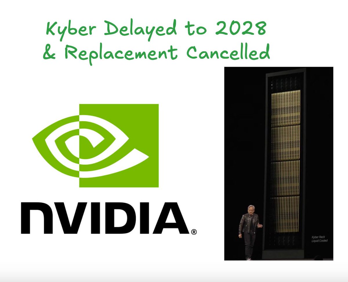
MASSIVE DELAY: Just 3 months after Jensen demoed Kyber NVL144 at GTC, it has faced major setbacks and has been delayed by more than 12 months, pushing it back to 2028. Below, we explain why Kyber has faced massive delays and why NVIDIA’s NVL72x2 back-to-back rack architecture was also cancelled, leaving Rubin Ultra with a limited scale-up domain. 👇️ 1/6🧵
8
17
197
101,381
bubble boi reposted
As the NVIDIA roadmap indicates, CPO NVSwitch will not be available until Feynman. As a result, NVIDIA currently has no proven solution to expand the scale-up world size for Rubin Ultra, leaving a gap for competitors like AMD MI500X or TPUv8i Broadfly to gain scale-up advantages over Rubin Ultra. 4/6🧵
5
8
161
49,864
Sorry I didn’t know I had to confirm all of you
Add me on WeChat
7
52
16,381
Nvidia’s motto is over promise and under deliver. Many saying this is bullish NPO (under the false premise that Kyber uses CPO) again just people pumping basket of stocks. What this is really telling you is just how poorly run this organization is and how they can’t execute on anything they promise.
MASSIVE DELAY: Just 3 months after Jensen demoed Kyber NVL144 at GTC, it has faced major setbacks and has been delayed by more than 12 months, pushing it back to 2028. Below, we explain why Kyber has faced massive delays and why NVIDIA’s NVL72x2 back-to-back rack architecture was also cancelled, leaving Rubin Ultra with a limited scale-up domain. 👇️ 1/6🧵
35
6
201
51,379
AI is pretty cooked tbh. Everyone going to ICML & NeurIPS these conferences are basically dead and just career fairs to buy out smart kids during their peak years and give them bullshit to work on so they don’t compete lol.
If I was a recent EE graduate I would probably go into power. I think the smartest career move you can do right now is do 2-3 years and a big data center power company like Eaton, Schneider Electric, or Flex learn the problem space and what customers want and start your own company. It isn’t as sexy as “AI” or “chip design” but we probably get more value out of new power architectures than chip design at this point.
16
15
690
83,181
If I was a recent EE graduate I would probably go into power. I think the smartest career move you can do right now is do 2-3 years and a big data center power company like Eaton, Schneider Electric, or Flex learn the problem space and what customers want and start your own company. It isn’t as sexy as “AI” or “chip design” but we probably get more value out of new power architectures than chip design at this point.
30
27
920
177,962
Man I need a new apartment the feng shui is oooooofff.
12
73
11,571
28-32 is peak engineer years after that you want to kys
The average age in Apollo 11 mission control was 28 btw.
17
4
723
54,989
10% of people bookmarked this
I interviewed @bubbleboi about his ratings of AI supply chain bottlenecks. We talked about DRAM, advanced packaging, CPO, HBF, PCBs, power delivery, etc. 0:00 HBM, DRAM, the cartel 7:24 Silicon photonics, CPO, Lumentum lasers 11:35 Advanced packaging: TSMC vs Intel 13:49 HBF: Sandisk/SK monopoly window 17:02 Memory accelerators TurboQuant 22:35 PCBs Unitika 27:27 Power: transition from 48V to 800V 31:32 Outsourced assembly test, fiber coupling 36:23 HBM vs DRAM vs NAND in 2-3 years 42:03 Where will hardware founders come from? 44:10 Alt accelerators: Etched, Taalas, MatX 48:43 Emerging tech: CPO bearishness 49:23 Hyperclouds 49:53 HBF timeline CXL 51:48 Voltage cooling wall 56:30 Rapid fire: Intel, Nvidia, TSMC, Alphabet 1:05:25 ASML, Hynix, Lumentum, Wolfspeed 1:13:25 Building conviction in Intel 1:19:37 Pitching Intel to funds 1:22:39 X accounts, analysts why care about any of this
4
14
279
60,278
Add me on WeChat
23
97
34,082
Instead of robots to pick up socks why don’t they make robots for agricultural and mining or is that just not like a big enough TAM yet?
92
9
515
70,316
Lmao no joke America just out innovates the entire world it’s kinda crazy. That plus a risk taking culture gets us a looooong way. The second point is key, because I’m sure if you discovered a room temperature super conductor or a way to get cheap scalable nuclear fusion in any other country it would still be next to impossible to raise capital to scale it. Meanwhile here you would get put in touch with Marc Andressen & Elon Musk within a week lol.
lee kuan yew on american culture
41
119
2,275
313,285
bubble boi reposted
You used to be allowed to do things in politics by age 20.
Ages of Founding Fathers in 1776: James Monroe, 18 Aaron Burr, 20 John Marshall, 20 Alexander Hamilton, 21 James Madison, 25 John Jay, 30 Thomas Jefferson, 33 Thomas Paine, 39 John Adams, 40 George Washington, 44 This nation was built by brilliant young men.
68
357
13,957
335,278
Man I love dogs so much
14
61
8,232