chips get all the love but the interconnects across all levels from c2c to rack-to-rack are as important, and many chip makers are sleeping on it until very recently. Even most interconnects people just want it to be as transparent as possible, just send and receive the bits with lower error rates and lower energy per bit, wrong long-term direction imo. Interconnects are part of the living creature, so many things happening in your blood vessels in addition to just moving stuff, and your axons do much more than carrying spikes.
People do not appreciate interconnects, smaller volume, poor margin, messy ecosystem, manual process, it's been a spiral of grinding, and it is largely invisible. How often do you see people tearing down transceivers and die shot of DSP chips vs logic chips? How often do you see high res pictures of all the connector's gold fingers on the NVL72 cartridge? Because it sounds boring, it's just making contacts, shoving electrons and photons, what a simple problem.
But that is deceiving, and theres so much to it. You might want 576 to begin with, had to cut down to 288, then to 144, and finally to 72, and that barely worked first time. You are entering the domain of analog and mixed signaling, you are fighting copper real estate with power delivery, you are getting impedance mismatch and reflections and interference at every stupid interfaces, your optical components' and connectors' backreflection is making your laser mode hop.. And we are not even going into the thermal and strain-stress, the reliability of how many times you can actually mate your connector, the horrible jobs people are doing across the stack from science-project-originated photonic PDKs to hand cleaved laser dies to optical engines to rack manufacturing, on spec-ing out the requirements, the tolerances.. On top of all these, people thinking about where the bits should be going and people who know what the bits have to go thru are two totally different groups of people.
But it is shifting, pluggable volumes shipped are doubling and tripling for scale-out, scale-up domain asks for much higher bw than scale-out, and interconnects are inevitable even if you cram as much compute and memory onto a single wafer. People will see it always has been interconnects, the chips people have already been doing it on the chips, that you can sort it out with your chip designers and foundries, and now you need to work with more people to sort it out from chips to boards/trays to racks to pods to data halls and data centers. These people speak very different languages and care about very different things, and it will take a lot of effort to pull order out of all the chaos.
At the end of the day, it is such a crazy problem to work on, such a beautiful thing to make, millions of amps of current flipping 1e20 of flops, sextillions of photons carrying thousands of terabits per second, a few tons of copper, tens of thousands of fibers totally few hundred kilometers, one scale-up domain. You absolutely need a group of people that appreciate the beauty and care about the craft behind the grinding to make it together.
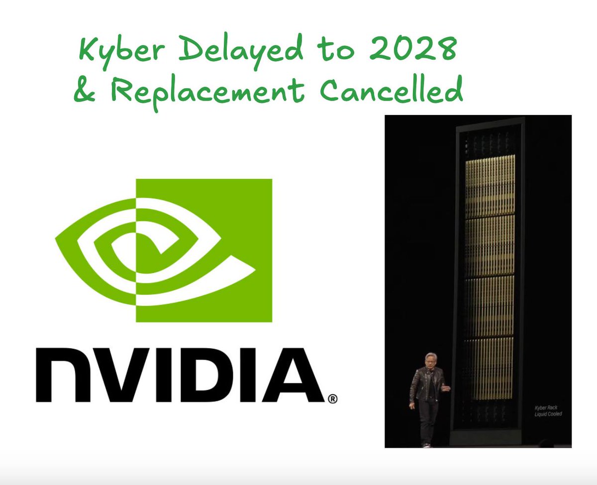
MASSIVE DELAY: Just 3 months after Jensen demoed Kyber NVL144 at GTC, it has faced major setbacks and has been delayed by more than 12 months, pushing it back to 2028. Below, we explain why Kyber has faced massive delays and why NVIDIA’s NVL72x2 back-to-back rack architecture was also cancelled, leaving Rubin Ultra with a limited scale-up domain. 👇️ 1/6🧵